M29W512B Ver la hoja de datos (PDF) - STMicroelectronics
Número de pieza
componentes Descripción
Fabricante
M29W512B Datasheet PDF : 18 Pages
| |||
M29W512B
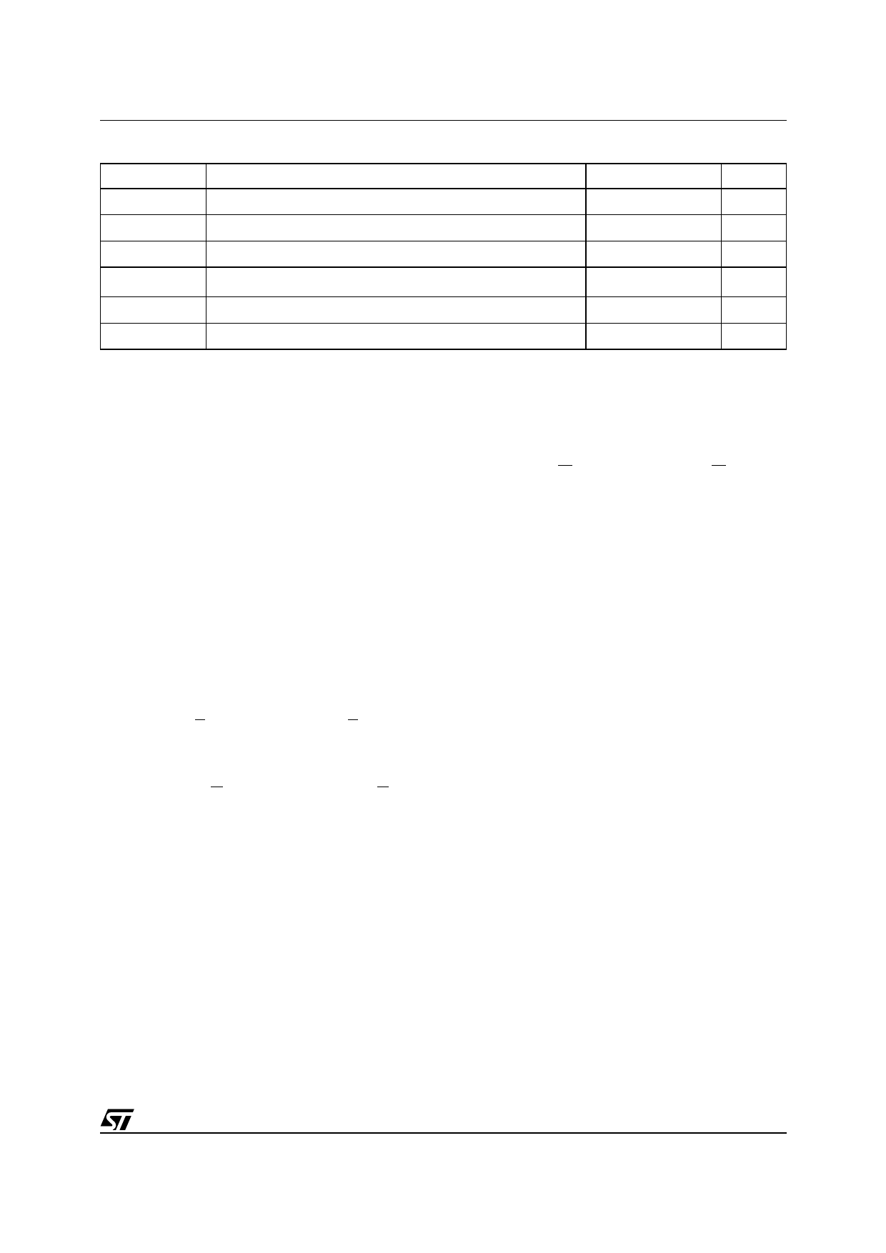
Table 2. Absolute Maximum Ratings (1)
Symbol
Parameter
Value
Unit
TA
Ambient Operating Temperature
0 to 70
°C
TBIAS
Temperature Under Bias
–50 to 125
°C
TSTG
Storage Temperature
–65 to 150
°C
VIO (2)
Input or Output Voltage
–0.6 to 4
V
VCC
Supply Voltage
–0.6 to 4
V
VID
Identification Voltage
–0.6 to 13.5
V
Note: 1. Except for the rating "Operating Temperature Range", stresses above those listed in the Table "Absolute Maximum Ratings" may
cause permanent damage to the device. These are stress ratings only and operation of the device at these or any other conditions
above those indicated in the Operating sections of this specification is not implied. Exposure to Absolute Maximum Rating condi-
tions for extended periods may affect device reliability. Refer also to the STMicroelectronics SURE Program and other relevant qual-
ity documents.
2. Minimum Voltage may undershoot to –2V during transition and for less than 20ns during transitions.
SIGNAL DESCRIPTIONS
See Figure 1, Logic Diagram, and Table 1, Signal
Names, for a brief overview of the signals connect-
ed to this device.
Address Inputs (A0-A15). The Address Inputs
select the cells in the memory array to access dur-
ing Bus Read operations. During Bus Write opera-
tions they control the commands sent to the
Command Interface of the internal state machine.
Data Inputs/Outputs (DQ0-DQ7). The Data In-
puts/Outputs output the data stored at the selected
address during a Bus Read operation. During Bus
Write operations they represent the commands
sent to the Command Interface of the internal state
machine.
Chip Enable (E). The Chip Enable, E, activates
the memory, allowing Bus Read and Bus Write op-
erations to be performed. When Chip Enable is
High, VIH, all other pins are ignored.
Output Enable (G). The Output Enable, G, con-
trols the Bus Read operation of the memory.
Write Enable (W). The Write Enable, W, controls
the Bus Write operation of the memory’s Com-
mand Interface.
VCC Supply Voltage. The VCC Supply Voltage
supplies the power for all operations (Read, Pro-
gram, Erase etc.).
The Command Interface is disabled when the VCC
Supply Voltage is less than the Lockout Voltage,
VLKO. This prevents Bus Write operations from ac-
cidentally damaging the data during power-up,
power-down and power surges. If the Program/
Erase Controller is programming or erasing during
this time then the operation aborts and the memo-
ry contents being altered will be invalid.
A 0.1µF capacitor should be connected between
the VCC Supply Voltage pin and the VSS Ground
pin to decouple the current surges from the power
supply. The PCB track widths must be sufficient to
carry the currents required during program and
erase operations, ICC3.
Vss Ground. The VSS Ground is the reference
for all voltage measurements.
3/18
Share Link: 