M25P80-VMW3 Ver la hoja de datos (PDF) - STMicroelectronics
Número de pieza
componentes Descripción
Fabricante
M25P80-VMW3 Datasheet PDF : 41 Pages
| |||
M25P80
Protection Modes
The environments where non-volatile memory de-
vices are used can be very noisy. No SPI device
can operate correctly in the presence of excessive
noise. To help combat this, the M25P80 boasts the
following data protection mechanisms:
■ Power-On Reset and an internal timer (tPUW)
can provide protection against inadvertant
changes while the power supply is outside the
operating specification.
■ Program, Erase and Write Status Register
instructions are checked that they consist of a
number of clock pulses that is a multiple of
eight, before they are accepted for execution.
■ All instructions that modify data must be
preceded by a Write Enable (WREN)
instruction to set the Write Enable Latch
(WEL) bit . This bit is returned to its reset state
by the following events:
– Power-up
– Write Disable (WRDI) instruction
completion
– Write Status Register (WRSR) instruction
completion
– Page Program (PP) instruction completion
– Sector Erase (SE) instruction completion
– Bulk Erase (BE) instruction completion
■ The Block Protect (BP2, BP1, BP0) bits allow
part of the memory to be configured as read-
only. This is the Software Protected Mode
(SPM).
■ The Write Protect (W) signal allows the Block
Protect (BP2, BP1, BP0) bits and Status
Register Write Disable (SRWD) bit to be
protected. This is the Hardware Protected
Mode (HPM).
■ In addition to the low power consumption
feature, the Deep Power-down mode offers
extra software protection from inadvertant
Write, Program and Erase instructions, as all
instructions are ignored except one particular
instruction (the Release from Deep Power-
down instruction).
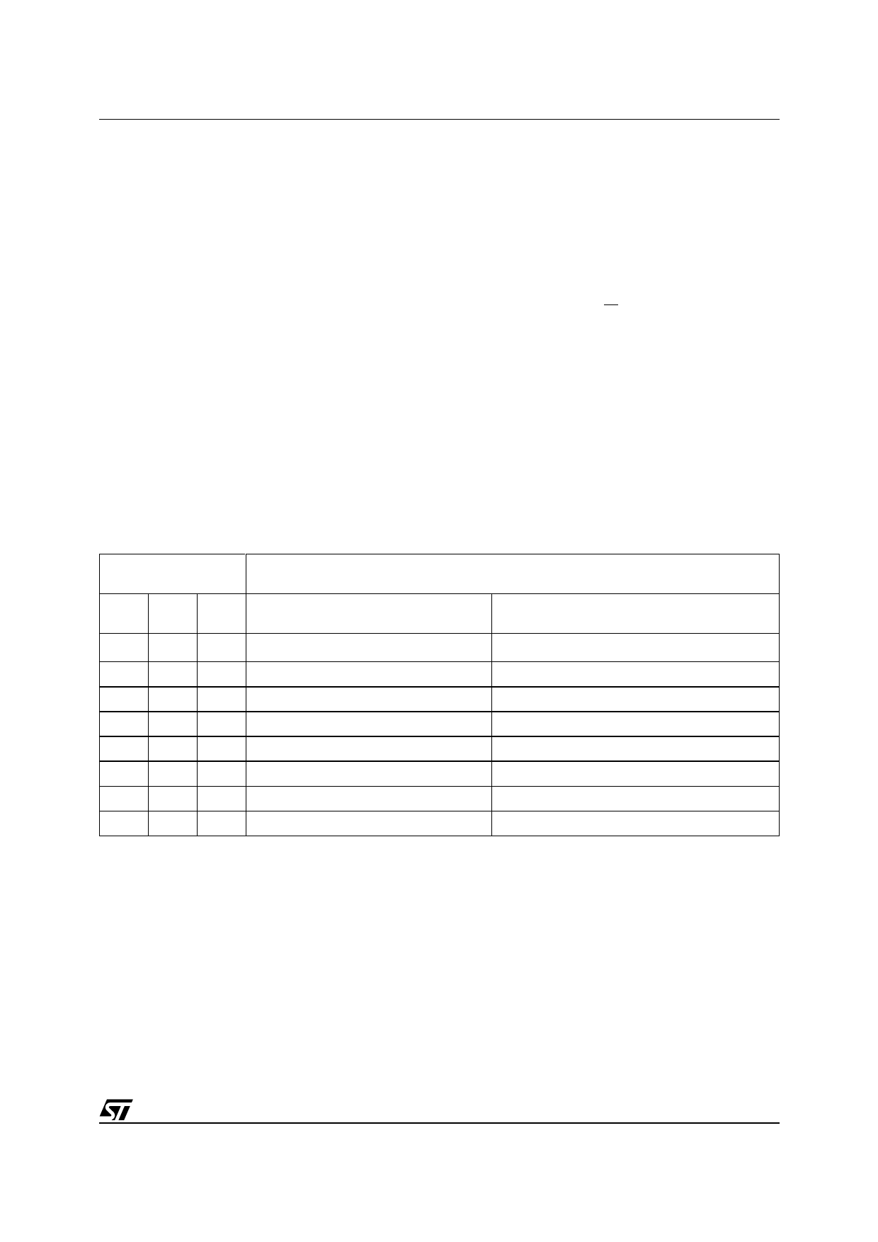
Table 2. Protected Area Sizes
Status Register
Content
Memory Content
BP2 BP1 BP0
Bit Bit Bit
Protected Area
Unprotected Area
0
0
0 none
All sectors1 (sixteen sectors: 0 to 15)
0
0
1 Upper sixteenth (Sector 15)
Lower fifteen-sixteenths (fifteen sectors: 0 to 14)
0
1
0 Upper eighth (two sectors: 14 and 15) Lower seven-eighths (fourteen sectors: 0 to 13)
0
1
1 Upper quarter (four sectors: 12 to 15)
Lower three-quarters (twelve sectors: 0 to 11)
1
0
0 Upper half (eight sectors: 8 to 15)
Lower half (eight sectors: 0 to 7)
1
0
1 All sectors (sixteen sectors: 0 to 15)
none
1
1
0 All sectors (sixteen sectors: 0 to 15)
none
1
1
1 All sectors (sixteen sectors: 0 to 15)
none
Note: 1. The device is ready to accept a Bulk Erase instruction if, and only if, all Block Protect (BP2, BP1, BP0) are 0.
9/41
Share Link: 