M24164-BN3 Ver la hoja de datos (PDF) - STMicroelectronics
Número de pieza
componentes Descripción
Fabricante
M24164-BN3 Datasheet PDF : 16 Pages
| |||
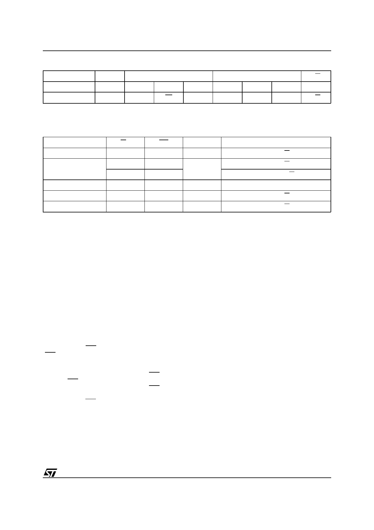
Table 3. Device Select Code
Chip Enable
Bit
b7
b6
b5
b4
Device Select
1
Note: The MSB b7 is sent first.
E2
E1
E0
M24164
MSB Address
RW
b3
b2
b1
b0
A10
A9
A8
RW
Table 4. Operating Modes (1)
Mode
RW bit
Current Address Read
’1’
’0’
Random Address Read
’1’
Sequential Read
’1’
Byte Write
’0’
Page Write
’0’
Note: 1. X = VIH or VIL.
WP
Data Bytes
Initial Sequence
X
1
START, Device Select, RW = ’1’
X
START, Device Select, RW = ’0’, Address,
1
X
reSTART, Device Select, RW = ’1’
X
≥1
As CURRENT or RANDOM Mode
VIL
1
START, Device Select, RW = ’0’
VIL
≤ 16
START, Device Select, RW = ’0’
SIGNAL DESCRIPTIONS
Serial Clock (SCL). The SCL input pin is used to
synchronize all data in and out of the memory. A
resistor can be connected from the SCL line to VCC
to act as a pull up (see Figure 3).
Serial Data (SDA). The SDA pin is bi-directional
and is used to transfer data in or out of the memory.
It is an open drain output that may be wire-OR’ed
with other open drain or open collector signals on
the bus. A resistor must be connected from the SDA
bus line to VCC to act as pull up (see Figure 3).
Chip Enable (E2 - E0). These chip enable inputs
are used to set 3 bits (b6, b5, b4) of the 7 bit device
select code. These inputs may be driven dynami-
cally or tied to VCC or VSS to establish the device
select code.
Write Control (WC). A hardware Write Control pin
(WC) is provided on pin 7 of the memory. This
feature is useful to protect the entire contents of the
memory from any erroneous erase/write cycle. The
Write Control signal is used to enable (WC=VIL) or
disable (WC=VIH) write instructions to the entire
memory area. When unconnected, the WC input is
internally read as VIL and write operations are
allowed. When WC=1, Device Select and Address
bytes are acknowledged, Data bytes are not ac-
knowledged.
Refer to Application Note AN404 for more detailed
information about Write Control feature.
DEVICE OPERATION
I2C Bus Background
The memory supports the I2C protocol. This proto-
col defines any device that sends data onto the bus
as a transmitter and any device that reads the data
as a receiver. The device that controls the data
transfer is known as the master and the other as
the slave. The master will always initiate a data
transfer and will provide the serial clock for syn-
chronisation. The memory is always a slave device
in all communications.
Start Condition. START is identified by a high to
low transition of the SDA line while the clock SCL
is stable in the high state. A START condition must
precede any command for data transfer. Except
during a programming cycle, the memory continu-
ously monitors the SDA and SCL signals for a
START condition and will not respond unless one
is given.
Stop Condition. STOP is identified by a low to high
transition of the SDA line while the clock SCL is
stable in the high state. A STOP condition termi-
nates communication between the memory and the
bus master. A STOP condition at the end of a Read
sequence, after and only after a No-Acknowledge,
forces the standby state. A STOP condition at the
end of a Write command triggers the internal
EEPROM write cycle.
3/16
Share Link: 