LX8587 Ver la hoja de datos (PDF) - Microsemi Corporation
Número de pieza
componentes Descripción
Fabricante
LX8587 Datasheet PDF : 11 Pages
| |||
LX8587x-xx
®
3A Low Dropout Positive Regulators
TM
PRODUCTION DATA SHEET
ABSOLUTE MAXIMUM RATINGS
Power Dissipation ................................................................................... Internally Limited
Input Voltage ................................................................................................................ 10V
Input to Output Voltage Differential............................................................................. 10V
Maximum Output Current............................................................................................... 5A
Maximum Operating Junction Temperature .............................................................. 150°C
Storage Temperature Range........................................................................ -65°C to 150°C
Peak Package Solder Reflow Temp. (40 seconds max. exposure) .................260°C (+0,-5)
Note: Exceeding these ratings could cause damage to the device. All voltages are with respect to
Ground. Currents are positive into, negative out of specified terminal.
THERMAL DATA
DD Plastic TO-263 3-Pin
THERMAL RESISTANCE-JUNCTION TO AMBIENT, θJA
THERMAL RESISTANCE-JUNCTION TO TAB, θJT
P Plastic TO-220 3-Pin
THERMAL RESISTANCE-JUNCTION TO AMBIENT, θJA
THERMAL RESISTANCE-JUNCTION TO TAB, θJT
DT Plastic TO-252 3-Pin
THERMAL RESISTANCE-JUNCTION TO AMBIENT, θJA
THERMAL RESISTANCE-JUNCTION TO TAB, θJT
60°C/W
2.7°C/W
60°C/W
2.7°C/W
60°C/W
2.7°C/W
Junction Temperature Calculation: TJ = TA + (PD x θJT).
The θJA & θJT numbers are guidelines for the thermal performance of the device/pc-board
system. All of the above assume no ambient airflow.
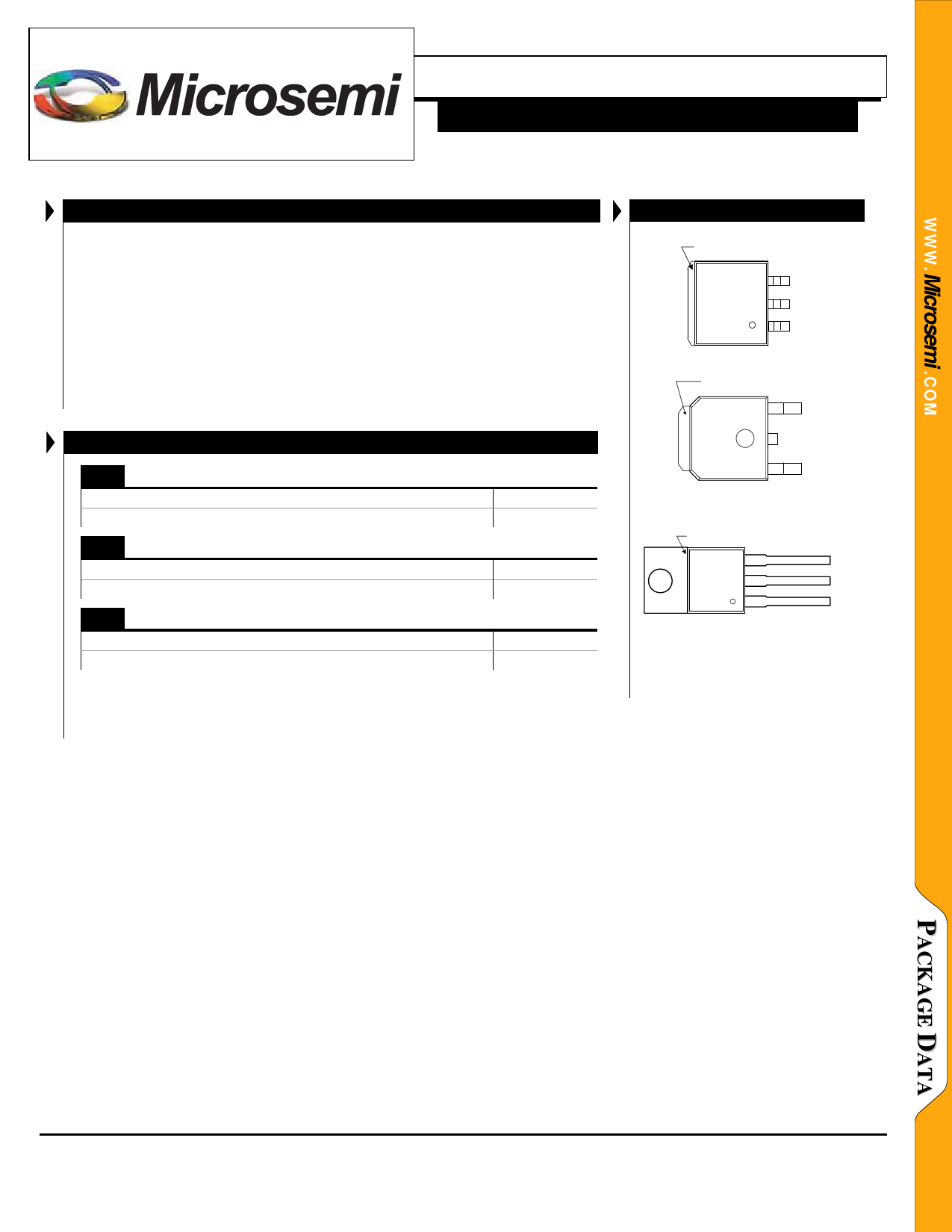
PACKAGE PIN OUT
TAB is VOUT
3
VIN
2
VOUT
1
ADJ /
GND*
DD PACKAGE (3-PIN)
(Top View)
TAB is VOUT
3
VIN
2
VOUT
ADJ/
1
GND
*
DT PACKAGE (3-PIN)
(Top View)
TAB is VOUT
3
2
1
P PACKAGE (3-PIN)
(Top View)
VIN
VOUT
ADJ /
GND*
*Pin 1 is GND for fixed voltage versions
RoHS 100% Matte Tin Lead Finish
Copyright © 2000
Rev. 2.0a, 2005-10-25
Microsemi
Integrated Products
11861 Western Avenue, Garden Grove, CA. 92841, 714-898-8121, Fax: 714-893-2570
Page 2
Share Link: 