LX1684CDT(2001) Ver la hoja de datos (PDF) - Microsemi Corporation
Número de pieza
componentes Descripción
Fabricante
LX1684CDT Datasheet PDF : 12 Pages
| |||
LINFINITY DIVISION
LX1684
Voltage-Mode PWM Controller
PRODUCTION
ABSOLUTE MAXIMUM RATINGS (NOTE 1)
Supply Voltage (VC1) ...................................................................................... 18V
Supply Voltage (VCC) ........................................................................................ 7V
Input Voltage (CSP Pin) .................................................................................. 14V
Output Drive Peak Current Source (500ns).................................................... 1.0A
Output Drive Peak Current Sink (500ns)........................................................ 1.0A
Input Voltage (SS/ENABLE Pin)...........................................................-0.3 to 6V
Operating Junction Temperature ..................................................................150°C
Storage Temperature ...................................................................-65°C to +150°C
Lead Temperature (Soldering 10 Seconds) ..................................................300°C
Note: Exceeding these ratings could cause damage to the device. All voltages are with respect to
Ground. Currents are positive into, negative out of specified terminal.
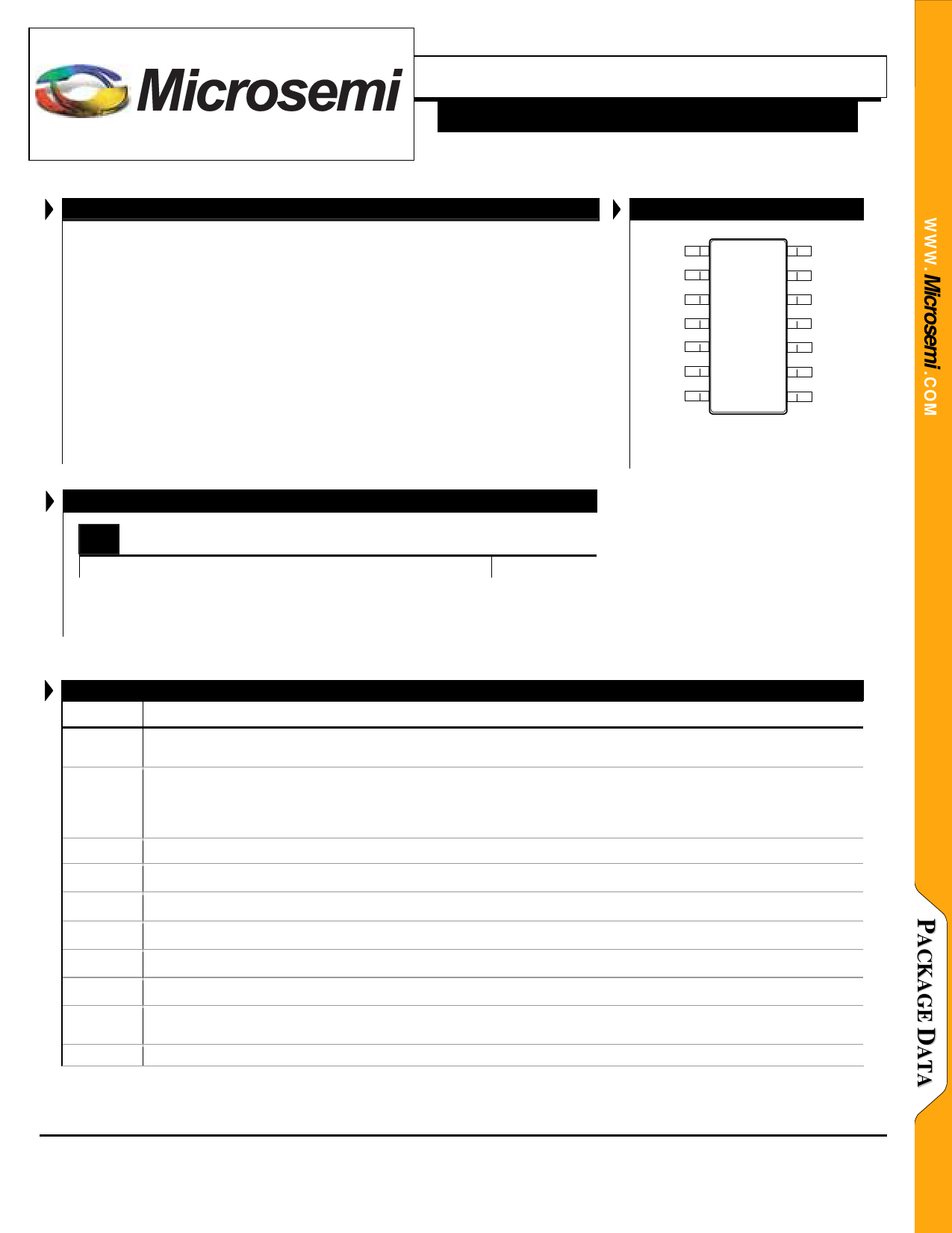
PACKAGE PIN OUT
FB
N/C
SS
VCSP
GND
PGND
BDRV
1
14
2
13
3
12
4
11
5
10
6
9
7
8
14-PIN SOIC
(Top View)
VCC
N/C
CS
N/C
VC1
N/C
TDRV
THERMAL DATA
D PACKAGE
THERMAL RESISTANCE-JUNCTION TO AMBIENT, θJA
165°C/W
Junction Temperature Calculation: TJ = TA + (PD x θJA).
The θJA numbers are guidelines for the thermal performance of the device/pc-board
system. All of the above assume no ambient airflow.
PIN NAME
VFB
SS
VCSP
GND
PGND
TDRV
BDRV
VC1
CS
VCC
FUNCTIONAL PIN DESCRIPTION
DESCRIPTION
Voltage Feedback. A 1.25V reference is connected to a resistor divider to set desired output voltage.
Soft-Start And Hiccup Capacitor Pin. During start up the voltage of this pin controls the output voltage. An
internal 22kΩ resistor and the external capacitor set the time constant for soft-startup. Soft-start does not begin
until the supply voltage exceeds the UVLO threshold. When over-current occurs, this capacitor is used for timing
hiccup. The PWM can be disabled by pulling the SS pin below 0.3V
Positive Over-Current Threshold Input
Analog ground for SS, FB, CS and VCC.
MOSFET driver power ground
Gate Drive For Upper MOSFET.
Gate Drive For Lower MOSFET.
Separate Supply For MOSFET Gate Drives. Connect to gate drive voltage.
Over-Current Set. Connect resistor between CS pin and the source of the upper MOSFET to set current-limit
point.
IC Supply Voltage (nominal 5V).
Copyright 2000
Rev. 1.0, 2001-09-19
Microsemi
Linfinity Microelectronics Division
11861 Western Avenue, Garden Grove, CA. 92841, 714-898-8121, Fax: 714-893-2570
Page 2
Share Link: 