LV4991M Ver la hoja de datos (PDF) - SANYO -> Panasonic
Número de pieza
componentes Descripción
Fabricante
LV4991M Datasheet PDF : 11 Pages
| |||
Cautions for use
LV4991M
1. Input coupling capacitor (C3)
The input coupling capacitor C3 and input resistor R1 make up the high-pass filter, attenuating the bass frequency.
Therefore, the capacitance value must be selected with due consideration of the pass band. Note with care that this
capacitance value affects the pop sound at startup.
Namely, the increased capacitance value will make the pop sound louder.
2. Pin 3 capacitor (C4)
This capacitor C4 is designed to reduce the power ripple. The ripple removal ratio increases when the capacitance is
larger. Note however that this capacitor affects the pop sound at startup.
Design must therefore be made by taking into both features as above described.
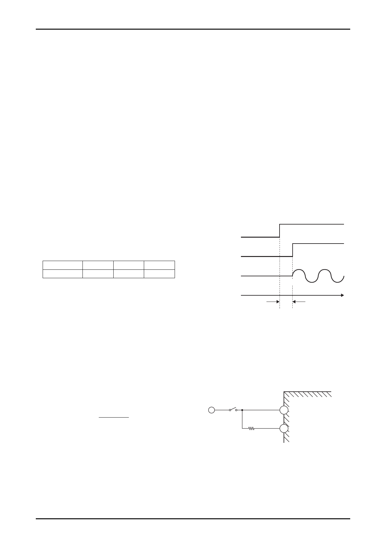
3. Pin 4 control (second amplifier stop control function)
Pin 4 is a pin to turn ON/OFF the operation of second amplifier. By using this function, the pop sound at startup can be
reduced. Note that pin 4 can be controlled by applying the voltage described below :
Second amplifier ON ⇒ V4 = 1.6 to VCCV or OPEN
Second amplifier OFF ⇒ V4 = 0 to 0.3V
When the pin-3 capacitor C4 is downsized, the pop sound becomes louder. The pop sound can be reduced by providing
the time Tmu to stop the second amplifier (see Fig. 1) while utilizing this function of the microcomputor. The
recommended mute time Tmu is as follows.
Pin 2:STBY
C4 [µF]
Tmu [ms]
0.1
≥ 170
0.22
≥ 270
0.33
≥ 280
Pin 4:CNT
Between pins 8 and 5:
OUT1-OUT2
AMP2:ON
Tmu
time
Fig. 1
4. Standby pin (pin 2)
By controlling the standby pin, the mode changeover can be made between standby and operation modes.
Standby mode ⇒ V2 = 0 to 0.3V
Operation mode ⇒ V2 = 1.9 to VCCV
When using the standby pin as interlocked with power supply as shown in Fig. 2, care should be taken because the
current ISTBY as expressed by the following equation flows through the standby pin.
ISTBY
=
VCC−1.4V
R3+21kΩ
VCC
VCC 7
R3 STBY 2
Fig. 2
No.A1492-6/11
Share Link: 