LTM4614 Ver la hoja de datos (PDF) - Linear Technology
N√∫mero de pieza
componentes Descripción
Fabricante
LTM4614 Datasheet PDF : 20 Pages
| |||
LTM4614
Pin Functions
Slave operation is performed by putting a resistor divider
from the master output to the ground, and connecting the
center point of the divider to this pin on the slave regulator.
If tracking is not desired, then connect the TRACK pin to
VIN. Load current must be present for tracking. See the
Applications Information section.
FB1, FB2 (L6, E6): The Negative Input of the Switching
Regulators’ Error Amplifier. Internally, these pins are con-
nected to VOUT with a 4.99k precision resistor. Different
output voltages can be programmed with an externally
connected resistor between the FB and GND pins. Two
power modules can current share when this pin is con-
nected in parallel with the adjacent module’s FB pin. See
the Applications Information section.
COMP1, COMP2 (L5, E5): Current Control Threshold
and Error Amplifier Compensation Point. The current
comparator threshold increases with this control voltage.
Two power modules can current share when this pin is
connected in parallel with the adjacent module’s COMP
pin. Each channel has been internally compensated. See
the Applications Information section.
PGOOD1, PGOOD2 (L4, E4): Output Voltage Power
Good Indicator. Open-drain logic output that is pulled to
ground when the output voltage is not within ±7.5% of
the regulation point.
RUN/SS1, RUN/SS2 (L2, E2): Run Control and Soft-Start
Pins. A voltage above 0.9V will turn on the module, and
below 0.6V will turn off the module. This pin has a 1M
resistor to VIN and a 1000pF capacitor to GND. The volt-
age on the RUN/SS pin clamps the control loop’s current
comparator threshold. A RUN/SS pin voltage of 2.375V
upon completion of soft-start guarantees the regulator can
deliver full output current. To turn off the module while
VIN remains active, the RUN/SS pin should be pulled low
with a falling edge ≤ 1µs to ensure the device does not
transition slowly through the internal undervoltage lockout
threshold. See Applications Information section for soft-
start information.
SW1, SW2 (H2-H6, B2-B6): The switching node of the
circuit is used for testing purposes. This can be connected
to copper on the board for improved thermal performance.
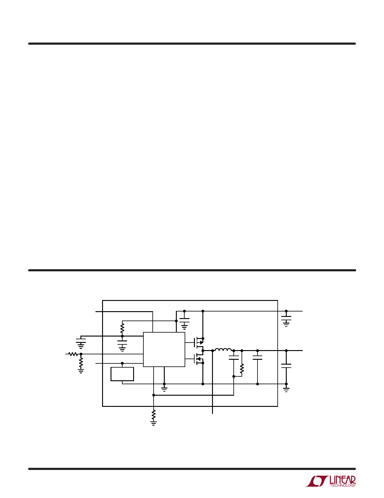
Simplified Block Diagram
PGOOD
TRACK 4.99k
SUPPLY
RUN/SS
CSSEXT
TRACK
5.76k
COMP
RSS
1M
CSS
1000pF
INTERNAL
COMP
CONTROL, DRIVE
POWER FETS
4.7µF
6.3V
M1 0.47µH
C2
M2 470pF
VIN
R1
4.99k
VOUT
4.7µF
6.3V
GND
VIN
22µF 2.375V TO 5.5V
6.3V
VOUT
1.5V
4A
100µF
X5R
FB
SW
RFB
5.76k
4614 F01
Figure 1. Simplified LTM4614 Block Diagram of Each Switching Regulator Channel
4614fb
6
Share Link: 