LTM10C348S Ver la hoja de datos (PDF) - Toshiba
Número de pieza
componentes Descripción
Fabricante
LTM10C348S Datasheet PDF : 10 Pages
| |||
TIMING SPECIFICATION 1)2) 3) 4)5)
LTM10C348S
Item
Frame Period
Vertical
Display Term
One Line Scanning
Time
Horizontal
Display Term
Clock Period
Symbol
t1
t2
t3
t4
t5
Min.
604 × t3
-
600 × t3
958 × t5
26.3
800 × t5
24.7
Typ.
628 × t3
16.58
600 × t3
1056 × t5
26.4
800 × t5
25.0
Max.
Unit
Remarks
677 × t3
-
17.86
ms
600 × t3
-
1064 × t5
-
µs
800 × t5
-
27.8
ns
Note 1) Refer to TIMING CHART and LVDS (DF90CF364MTD) specifications by National Semiconductor.
Note 2) If ENAB is fixed to "H" or "L" level for certain period while NCLK is supplied, the panel displays black with some
flicker.
Note 3) If NCLK is fixed to "H" or "L" level for certain period while ENAB is supplied, the panel may be damaged.
Note 4) Please adjust LCD operating signal timing and FL driving frequency, to optimize the display quality.
There is a possibility that flicker is observed by the interference of LCD operating signal timing and FL driving
Condition (especially driving frequency ), even if the condition satisfies above timing specifications and
recommended operating conditions shown in 3.
Note 5) Do not make t1,t2 and t3 fluctuate.
If t1,t2 and t3 are fluctuate, the panel displays black.
Notes 6) Do not hold NCLK on “H” level nor “L” level during VDD(+3.3V) Is supplied. When it holds on, DC voltage
supplies to liquid crystal materials and it may cause damage to liquid crystal materials.
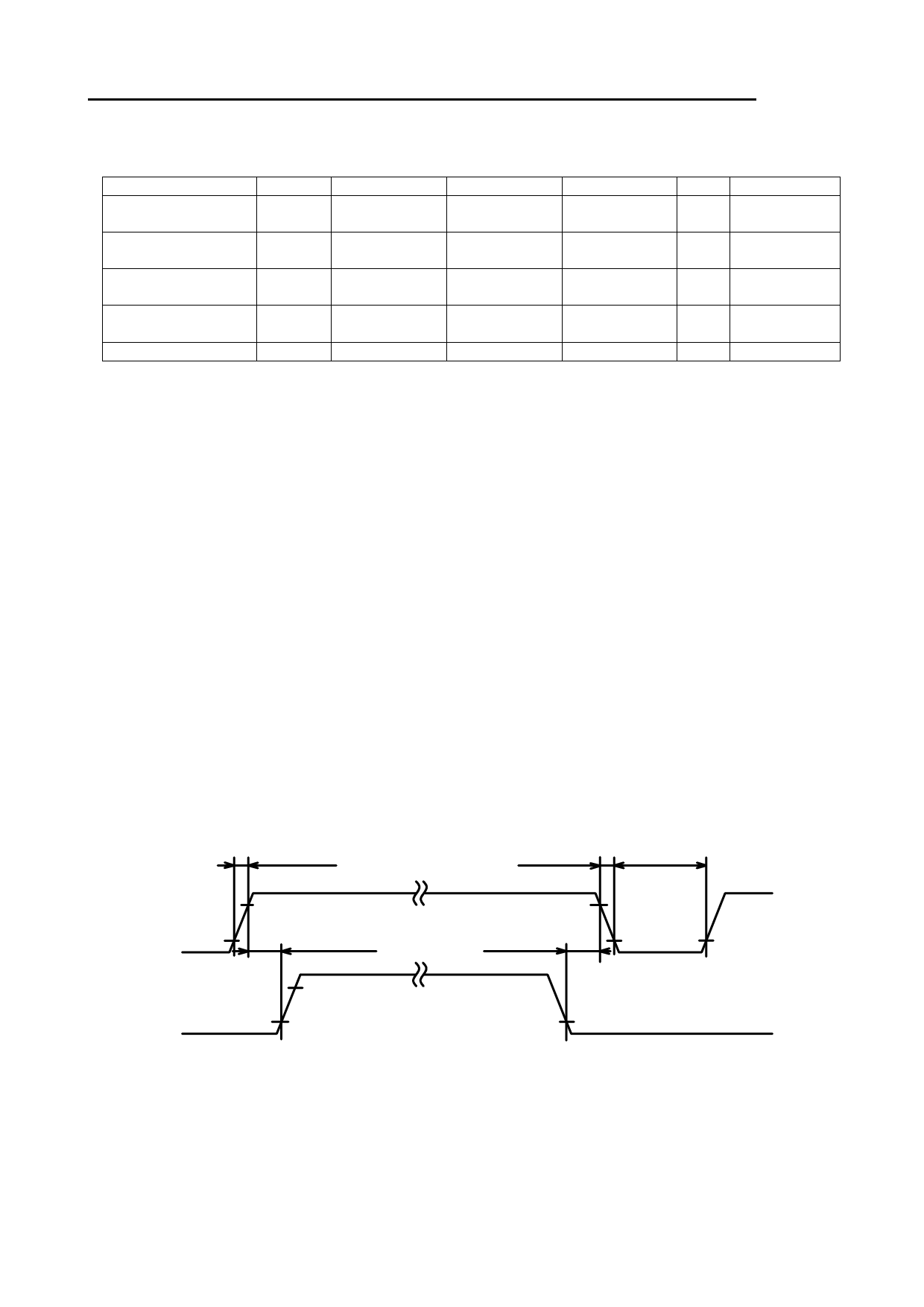
SEQUENCE OF POWER SUPPLIES AND SIGNALS
10ms(Max.)
10ms(Max.) 500ms(Min.)
3.0V
VDD 0.2V
40ms(Max.)
0ms(Min.)
NCLK
ENAB
DATA
0 . 2V DD
3.0V
40ms(Max.)
0ms(Min.)
0.2V
0.2V
0 . 2V DD
(5/10)
2000-02-18 (Ver.2.4)
Share Link: 