LTC6603 Ver la hoja de datos (PDF) - Linear Technology
Número de pieza
componentes Descripción
Fabricante
LTC6603 Datasheet PDF : 24 Pages
| |||
LTC6603
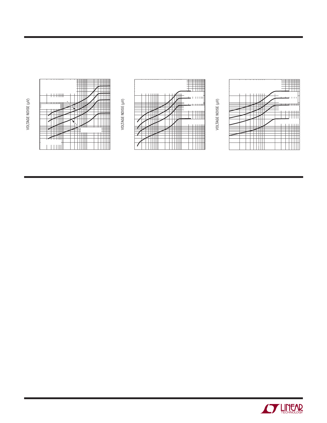
TYPICAL PERFORMANCE CHARACTERISTICS
Integral Input Referred Noise
1000
VS = 3V, RBIAS = 30.9k
LPF1 = 1,BW = 2.5MHz
TA = 25°C
GAIN = 6dB
100
GAIN = 0dB
10
GAIN = 12dB
GAIN = 24dB
1
10k
100k
1M
INTEGRATION BW (Hz)
10M
6603 G33
Integral Input Referred Noise
1000
VS = 3V, RBIAS = 30.9k
LPF1 = 0, LPF0 = 1, BW = 625kHz
TA = 25°C
GAIN = 0dB
100
GAIN = 6dB
GAIN = 12dB
GAIN = 24dB
10
1
10k
100k
1M
10M
INTEGRATION BW (Hz)
6603 G34
Integral Input Referred Noise
1000
VS = 3V, RBIAS = 30.9k
LPF1 = LPF0 = 0, BW = 156.25kHz
TA = 25°C
GAIN = 0dB
100
GAIN = 6dB
GAIN = 12dB
GAIN = 24dB
10
1
10k
100k
1M
INTEGRATION BW (Hz)
6603 G35
PIN FUNCTIONS
V+IN (Pin 1): Input Voltage Supply (2.7V ≤ V ≤ 5.5V). This
supply must be kept free from noise and ripple. It should
be bypassed directly to a ground plane with a 0.1μF ca-
pacitor unless it is tied to V+A (Pin 2). The bypass should
be as close as possible to the IC, but is not as critical as
the bypassing of V+A and V+D (Pin16).
V+A (Pin 2): Analog Voltage Supply (2.7V ≤ V ≤ 3.6V). This
supply must be kept free from noise and ripple. It should be
bypassed directly to a ground plane with a 0.1μF capacitor.
The bypass should be as close as possible to the IC.
VOCM (Pin 3): Output common mode voltage reference. If
floated, an internal resistive divider sets the voltage on this
pin to half the supply voltage (typically 1.5V), maximiz-
ing the dynamic range of the filter. If this pin is floated, it
must be bypassed with a quality 1μF capacitor to ground.
This pin has a typical input impedance of 3.4k and may
be overdriven. Driving this pin to a voltage other than the
default value will reduce the signal range the filter can
handle before clipping.
RBIAS (Pin 4): Oscillator Frequency-Setting Resistor Input.
The value of the resistor connected between this pin and
ground determines the frequency of the master oscillator,
and sets the bias currents for the filter networks. The voltage
on this pin is held by the LTC6603 to approximately 1.17V.
For best performance, use a precision metal film resis-
tor with a value between 30.9k and 200k and limit the
capacitance on this pin to less than 10pF. This resistor is
necessary even if an external clock is used.
CLKCNTL (Pin 5): Clock Control Input. This three-state
input selects the function of CLKIO (Pin 15). Tying the
CLKCNTL pin to ground allows the CLKIO pin to be driven
by an external clock (CLKIO is the master clock input).
If the CLKCNTL pin is floated, the internal oscillator is
enabled, but the master clock is not present at the CLKIO
pin (CLKIO is a no-connect). If the CLKCNTL pin is tied
to V+D (Pin 16), the internal oscillator is enabled and the
master clock is present at the CLKIO pin (CLKIO is the
master clock output). To detect a floating CLKCNTL pin,
the LTC6603 attempts to pull the pin toward mid-supply.
This is realized with two internal 15μA current sources, one
tied to V+D and CLKCNTL and the other one tied to ground
and CLKCNTL. Therefore, driving the CLKCNTL pin high
requires sourcing approximately 15μA. Likewise, driving
the CLKCNTL pin low requires sinking 15μA. When the
CLKCNTL pin is floated, it should be bypassed by a 1nF
capacitor to ground or be surrounded by a ground shield
to prevent excessive coupling from other PCB traces.
6603f
10
Share Link: 