LTC5536 Ver la hoja de datos (PDF) - Linear Technology
Número de pieza
componentes Descripción
Fabricante
LTC5536 Datasheet PDF : 12 Pages
| |||
LTC5536
PI FU CTIO S
RFIN (Pin 1): RF Input Voltage. Referenced to VCC. A
coupling capacitor must be used to connect to the RF
signal source. The frequency range is 600MHz to 7GHz.
This pin has an internal 500Ω termination, an internal
Schottky diode detector and a peak detector capacitor.
GND (Pin 2): Ground.
VM (Pin 3): Comparator Negative Input. Apply reference
voltage to this pin.
LEN (Pin 4): Latch Enable Input. Output is latched when
LEN is high and transparent when LEN is low.
VOUT (Pin 5): Comparator Output.
VCC (Pin 6): Power Supply Voltage, 2.7V to 5.5V.
VCC should be bypassed appropriately with ceramic
capacitors.
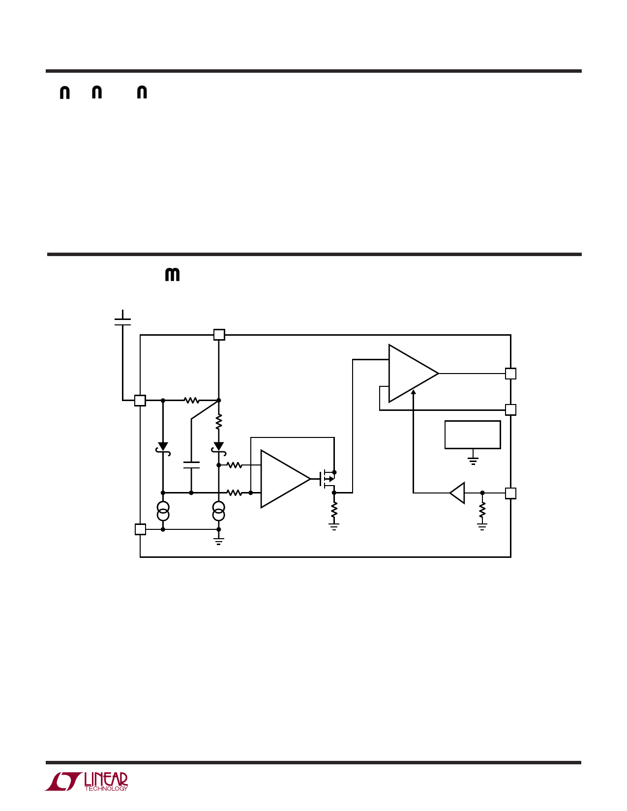
BLOCK DIAGRA
RFSOURCE
12pF TO 200pF
(DEPENDING ON
VCC
APPLICATION)
6
1
RFIN
500Ω
500Ω
GND 2
7.5k
15pF
7.5k
50µA
50µA
+
RF DET
–
+
COMP
–
VP
100mV
DC BIAS
10k
5 VOUT
BIAS
3 VM
4 LEN
110k
5536 BD
5536f
7
Share Link: 