LTC4218CGN-TRPBF(RevB) Ver la hoja de datos (PDF) - Linear Technology
Número de pieza
componentes Descripción
Fabricante
LTC4218CGN-TRPBF Datasheet PDF : 16 Pages
| |||
LTC4218
APPLICATIONS INFORMATION
The typical LTC4218 application is in a high availability
system that uses a positive voltage supply to distribute
power to individual cards. The basic application circuit
is shown in Figure 1. External component selection is
discussed in detail in the following sections.
RS
Q1
12V
2mΩ Si7108DN
VOUT
12V
3A
R1
10Ω
R2
224k
R3
20k
SENSE– GATE SOURCE
SENSE+
VDD
R4
140k
FB
UV
FLT LTC4218GN
OV
R5
PG
20k
ISET
RGATE
1k
CGATE
0.01μF
R6
150k
12V
R7
20k
R8
10k
RSET
20k
CT
0.1μF
C1
0.1μF
TIMER
INTVCC GND
IMON
RMON
20k
+
CL
330μF
ADC
4218 F01
Figure 1. 3A, 12V Card Resident Application
Turn-On Sequence
The power supply on a board is controlled by placing
an external N-channel pass transistor (Q1) in the power
path. Note the sense resistor (RS) detects current and
the capacitor (CGATE) controls gate slew rate. Resistor R1
prevents high frequency oscillations in Q1 and resistor
RGATE isolates CGATE during fast turn-off.
Several conditions must be present before the external
pass transistor can be turned on. First, the supply VDD
must exceed its undervoltage lockout level. Next, the
internally generated supply INTVCC must cross its 2.65V
undervoltage threshold. This generates a 25μs power-
on-reset pulse which clears the logic’s fault register and
initializes internal latches.
After the power-on-reset pulse, the LTC4218 will go through
the following sequence. First, the UV and OV pins must
indicate that the input power is within the acceptable range.
All of these conditions must be satisfied for a duration
of 100ms to ensure that any contact bounce during the
insertion has ended.
The pass transistor is turned on by charging up the GATE
with a 24μA charge pump generated current source
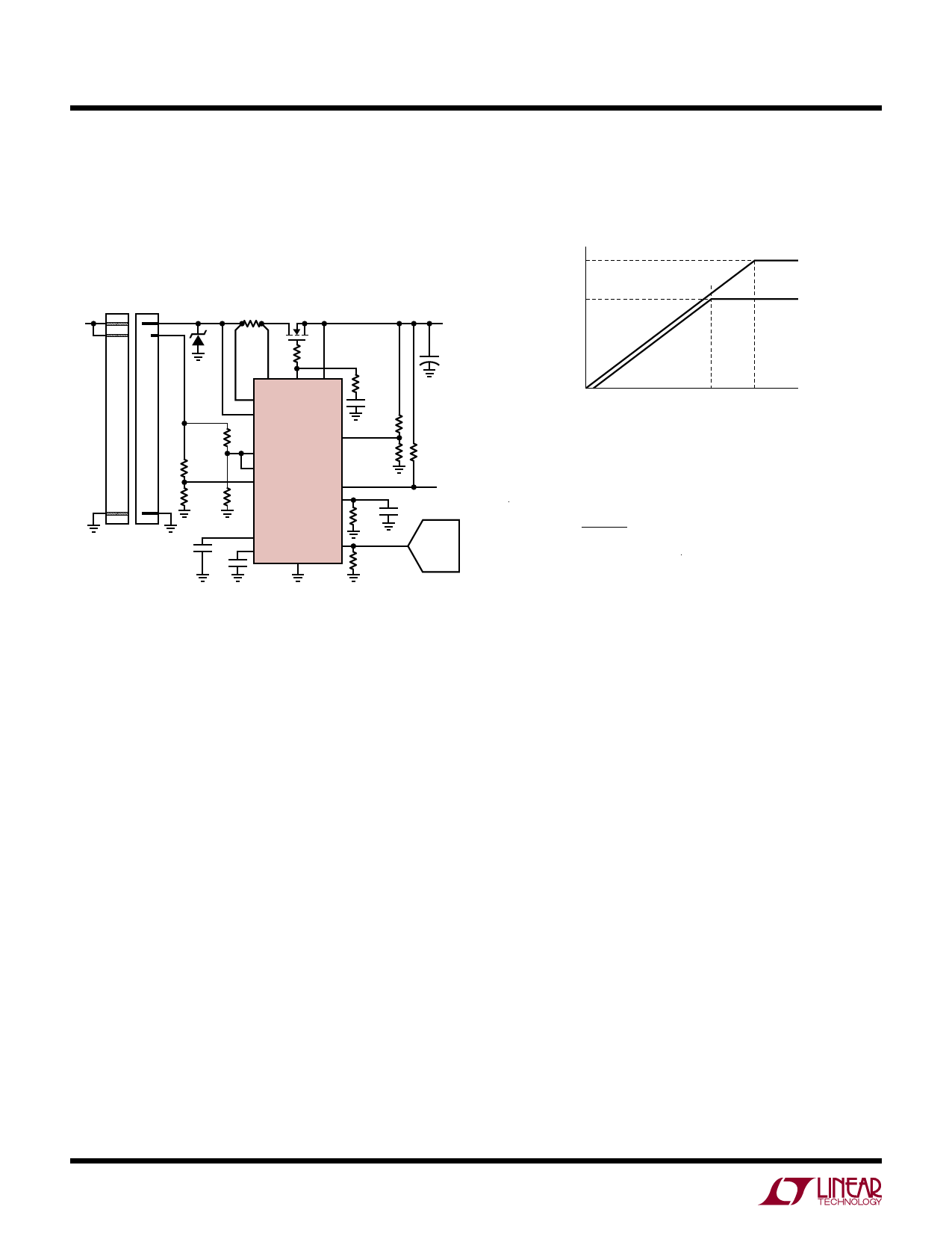
(Figure 2).
VDD + 6.15
VDD
SLOPE = 24μA/CGATE
GATE
SOURCE
t1
t2
4218 F02
Figure 2. Supply Turn-On
The voltage at the GATE pin rises with a slope equal to
24μA/CGATE and the supply inrush current is set at:
IINRUSH
=
CL
CGATE
• 24µA
When the GATE voltage reaches the MOSFET threshold
voltage, the switch begins to turn on and the SOURCE
voltage follows the GATE voltage as it increases. Once
SOURCE reaches VDD, the GATE will ramp up until clamped
by the 6.15V zener between GATE and SOURCE.
As the SOURCE pin voltage rises, so will the FB pin which
is monitoring it. If the voltage across the current sense
resistor (RS) gets too high, the inrush current will be limited
by the internal current limiting circuitry. Once the FB pin
crosses its 1.235V threshold and the GATE to SOURCE
voltage exceeds 4.2V, the PG pin will cease to pull low and
indicate that the power is good.
Turn-Off Sequence
The switch can be turned off by a variety of conditions. A
normal turn-off is initiated by the UV pin going below its
1.235V threshold. Additionally, several fault conditions will
turn off the switch. These include an input overvoltage (OV
pin) and overcurrent circuit breaker (SENSE pin). Normally,
the switch is turned off with a 250μA current pulling down
the GATE pin to ground. With the switch turned off, the
SOURCE pin voltage drops which pulls the FB pin below
4218fb
10
Share Link: 