LTC3707-SYNC Ver la hoja de datos (PDF) - Linear Technology
Número de pieza
componentes Descripción
Fabricante
LTC3707-SYNC Datasheet PDF : 32 Pages
| |||
LTC3707-SYNC
ABSOLUTE AXI U RATI GS
(Note 1)
Input Supply Voltage (VIN).........................30V to – 0.3V
Top Side Driver Voltages
(BOOST1, BOOST2) ...................................36V to – 0.3V
Switch Voltage (SW1, SW2) .........................30V to – 5V
INTVCC, EXTVCC, RUN/SS1, RUN/SS2, (BOOST1-SW1),
(BOOST2-SW2), PGOOD .............................7V to – 0.3V
SENSE1+, SENSE2 +, SENSE1–,
SENSE2 – Voltages ........................ (1.1)INTVCC to – 0.3V
PLLIN, PLLFLTR, FCB, Voltage ............ INTVCC to – 0.3V
ITH1, ITH2, VOSENSE1, VOSENSE2 Voltages ... 2.7V to – 0.3V
Peak Output Current <10µs (TG1, TG2, BG1, BG2) ... 3A
INTVCC Peak Output Current ................................ 40mA
Operating Temperature Range
LTC3707EGN-SYNC (Note 2) ............. – 40°C to 85°C
Junction Temperature (Note 3) ............................. 125°C
Storage Temperature Range ................. – 65°C to 150°C
Lead Temperature (Soldering, 10 sec).................. 300°C
UW U
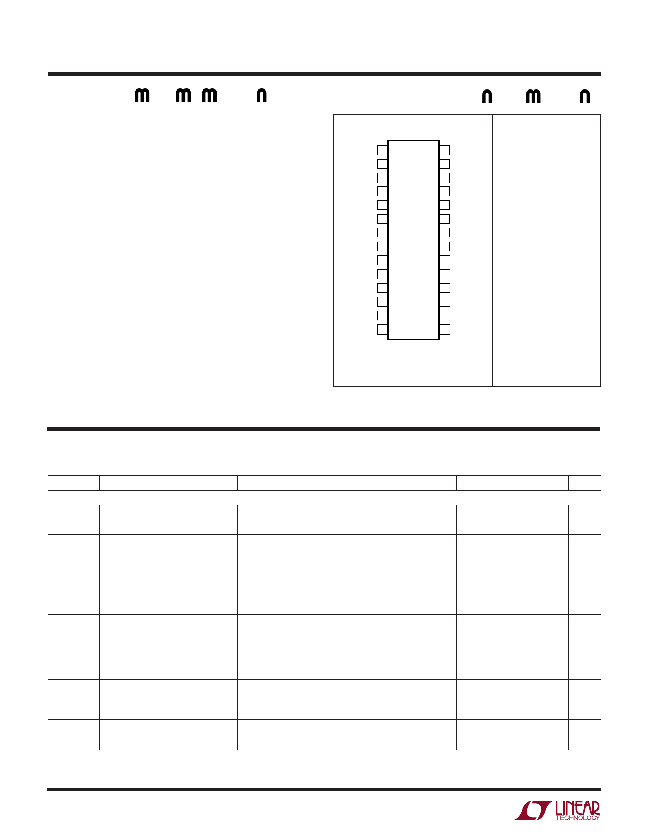
PACKAGE/ORDER I FOR ATIO
RUN/SS1 1
SENSE1+ 2
SENSE1– 3
VOSENSE1 4
PLLFLTR 5
PLLIN 6
FCB 7
ITH1 8
SGND 9
3.3VOUT 10
ITH2 11
VOSENSE2 12
SENSE2– 13
SENSE2+ 14
TOP VIEW
28 PGOOD
27 TG1
26 SW1
25 BOOST1
24 VIN
23 BG1
22 EXTVCC
21 INTVCC
20 PGND
19 BG2
18 BOOST2
17 SW2
16 TG2
15 RUN/SS2
GN PACKAGE
28-LEAD PLASTIC SSOP
TJMAX = 125°C, θJA = 95°C/W
ORDER PART
NUMBER
LTC3707EGN-SYNC
Consult LTC Marketing for parts specified with wider operating temperature ranges.
ELECTRICAL CHARACTERISTICS The q denotes the specifications which apply over the full operating
temperature range, otherwise specifications are at TA = 25°C. VIN = 15V, VRUN/SS1, 2 = 5V unless otherwise noted.
SYMBOL PARAMETER
CONDITIONS
MIN TYP MAX UNITS
Main Control Loops
VOSENSE1, 2
IVOSENSE1, 2
VREFLNREG
VLOADREG
Regulated Feedback Voltage
Feedback Current
Reference Voltage Line Regulation
Output Voltage Load Regulation
gm1, 2
gmGBW1, 2
IQ
VFCB
IFCB
VBINHIBIT
Transconductance Amplifier gm
Transconductance Amplifier GBW
Input DC Supply Current
Normal Mode
Shutdown
Forced Continuous Threshold
Forced Continuous Pin Current
Burst Inhibit (Constant Frequency)
Threshold
(Note 4); ITH1, 2 Voltage = 1.2V
(Note 4)
VIN = 3.6V to 30V (Note 4)
(Note 4)
Measured in Servo Loop; ∆ITH Voltage = 1.2V to 0.7V
Measured in Servo Loop; ∆ITH Voltage = 1.2V to 2.0V
ITH1, 2 = 1.2V; Sink/Source 5uA; (Note 4)
ITH1, 2 = 1.2V; (Note 4)
(Note 5)
VIN = 15V; EXTVCC Tied to VOUT1; VOUT1 = 5V
VRUN/SS1, 2 = 0V, VSTBYMD = Open;
VFCB = 0.85V
Measured at FCB pin
q 0.788
q
q
q 0.76
– 0.30
0.800
–5
0.002
0.1
– 0.1
1.3
3
350
20
0.800
– 0.18
4.3
0.812
– 50
0.02
0.5
– 0.5
35
0.84
– 0.1
4.8
V
nA
%/V
%
%
mmho
MHz
µA
µA
V
µA
V
UVLO
Undervoltage Lockout
VIN Ramping Down
q
3.5
4
V
VOVL
Feedback Overvoltage Lockout
Measured at VOSENSE1, 2
q 0.84 0.86 0.88
V
ISENSE
Sense Pins Total Source Current
(Each Channel); VSENSE1–, 2– = VSENSE1+, 2+ = 0V
– 90 – 60
µA
3707sf
2
Share Link: 