LTC2053I(RevB) Ver la hoja de datos (PDF) - Linear Technology
Número de pieza
componentes Descripción
Fabricante
LTC2053I
(Rev.:RevB)
(Rev.:RevB)
Linear Technology

LTC2053I Datasheet PDF : 16 Pages
| |||
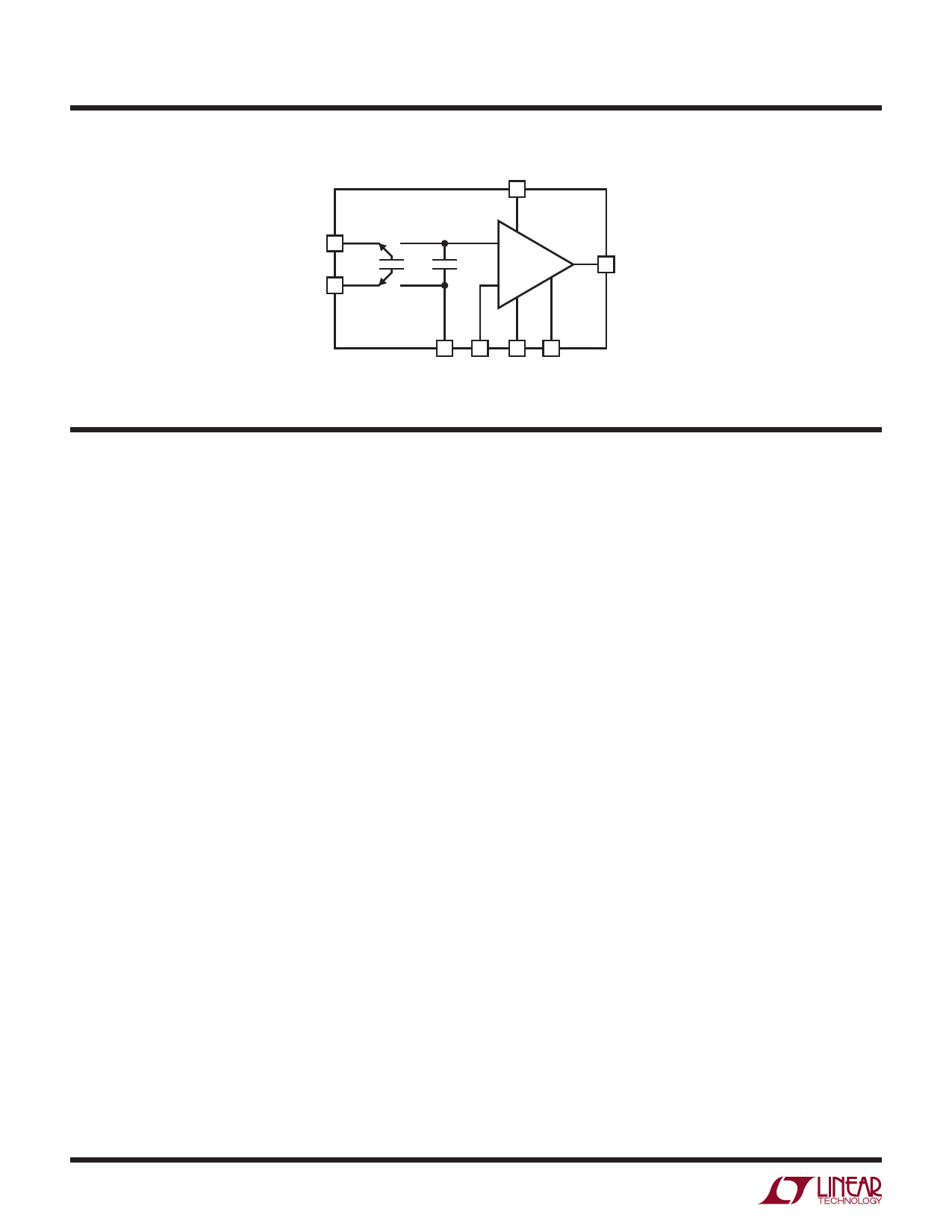
LTC2053/LTC2053-SYNC
APPLICATIO S I FOR ATIO
Settling Time
The sampling rate is 3kHz and the input sampling period
during which CS is charged to the input differential voltage
VIN is approximately 150µs. First assume that on each
input sampling period, CS is charged fully to VIN. Since CS
= CH (= 1000pF), a change in the input will settle to N bits
of accuracy at the op amp noninverting input after N clock
cycles or 333µs(N). The settling time at the OUT pin is also
affected by the settling of the internal op amp. Since the
gain bandwidth of the internal op amp is typically 200kHz,
the settling time is dominated by the switched capacitor
front end for gains below 100 (see Typical Performance
Characteristics).
Input Current
Whenever the differential input VIN changes, CH must be
charged up to the new input voltage via CS. This results in
an input charging current during each input sampling
period. Eventually, CH and CS will reach VIN and, ideally,
the input current would go to zero for DC inputs.
In reality, there are additional parasitic capacitors which
disturb the charge on CS every cycle even if VIN is a DC
voltage. For example, the parasitic bottom plate capacitor
on CS must be charged from the voltage on the REF pin to
the voltage on the –IN pin every cycle. The resulting input
charging current decays exponentially during each input
sampling period with a time constant equal to RSCS. If the
voltage disturbance due to these currents settles before
the end of the sampling period, there will be no errors
due to source resistance or the source resistance mis-
match between –IN and +IN. With RS less than 10k, no
DC errors occur due to this input current.
In the Typical Performance Characteristics section of this
data sheet, there are curves showing the additional error
from non-zero source resistance in the inputs. If there are
no large capacitors across the inputs, the amplifier is less
sensitive to source resistance and source resistance mis-
match. When large capacitors are placed across the in-
puts, the input charging currents described above result in
larger DC errors, especially with source resistor mis-
matches.
Power Supply Bypassing
The LTC2053 uses a sampled data technique and therefore
contains some clocked digital circuitry. It is therefore
sensistive to supply bypassing. For single or dual supply
operation, a 0.1µF ceramic capacitor must be connected
between Pin 8 (V+) and Pin 4 (V–) with leads as short as
possible.
10
SINGLE SUPPLY, UNITY GAIN
5V
8
V+IN + 3 +
V–IN V–D 2 –
4
7
6
5
0V < V+IN < 5V
0V < V–IN < 5V
0V < VD < 3.7V
VOUT = VD
DUAL SUPPLY
5V
8
V+IN + 3 +
VOUT
V–IN
V–D 2
–
4
–5V
7
6 R2
5
R1
VREF
VOUT
–5V < V–IN < 5V AND ⏐V–IN – VREF⏐ < 5.5V
–5V < V+IN < 5V AND ⏐V+IN – VREF⏐ < 5.5V
–5V < VD + VREF < 3.7V
( )R2
VOUT = 1 +
VD + VREF
R1
2053 F01
Figure 1
2053syncfb
Share Link: