LTC1404(RevA) Ver la hoja de datos (PDF) - Linear Technology
Número de pieza
componentes Descripción
Fabricante
LTC1404 Datasheet PDF : 24 Pages
| |||
LTC1404
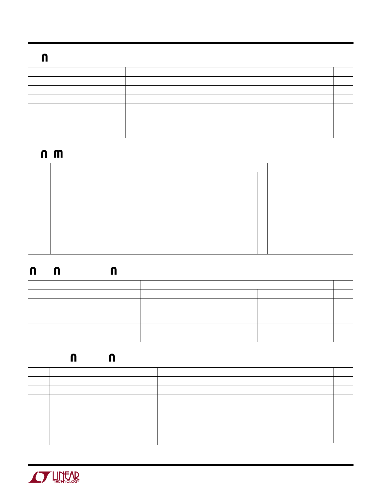
CO VERTER CHARACTERISTICS The ● denotes specifications which apply over the full operating temperature
range, unless otherwise noted specifications are at TA = 25°C. With internal reference VCC = 5V, fSAMPLE = 600kHz, tr = tf = 5ns, unless
otherwise specified (Note 6).
PARAMETER
CONDITIONS
MIN TYP MAX UNITS
Resolution (No Missing Codes)
● 12
Bits
Integral Linearity Error
(Note 7)
●
±1
LSB
Differential Linearity Error
●
±1
LSB
Offset Error
(Note 8)
±6
LSB
●
±8
LSB
Full-Scale Error
± 15
LSB
Full-Scale Tempco
IOUT(REF) = 0
●
±10 ±45 ppm/°C
DY A IC ACCURACY The ● denotes specifications which apply over the full operating temperature range, unless
otherwise noted specifications are at TA = 25°C. VCC = 5V, VSS = –5V, fSAMPLE = 600kHz.
SYMBOL PARAMETER
S/(N + D) Signal-to-Noise
THD
Total Harmonic Distortion
Up to 5th Harmonic
Peak Harmonic or
Spurious Noise
IMD
Intermodulation Distortion
Full Power Bandwidth
Full Linear Bandwidth (S/(N + D) ≥ 68dB)
CONDITIONS
100kHz Input Signal
300kHz Input Signal
100kHz Input Signal
300kHz Input Signal
100kHz Input Signal
300kHz Input Signal
fIN1 = 99.17kHz, fIN2 = 102.69kHz
fIN1 = 298.68kHz, fIN2 = 304.83kHz
MIN TYP MAX UNITS
● 69
72
dB
72
dB
●
– 82 – 76
dB
– 80
dB
●
– 84 – 76
dB
– 82
dB
– 82
dB
– 70
dB
5
MHz
1
MHz
UU
U
I TER AL REFERE CE CHARACTERISTICS The ● denotes specifications which apply over the full
operating temperature range, unless otherwise noted specifications are at TA = 25°C. VCC = 5V, fSAMPLE = 600kHz, tr = tf = 5ns, unless
otherwise specified.
PARAMETER
VREF Output Voltage
VREF Output Tempco
VREF Line Regulation
VREF Load Regulation
VREF Wake-Up Time from Sleep Mode
CONDITIONS
IOUT = 0
IOUT = 0
4.75V ≤ VCC ≤ 5.25V
– 5.25V ≤ VSS ≤ 0V
0 ≤ ⏐IOUT⏐ ≤ 1mA
CVREF = 10µF
MIN
2.410
●
TYP
2.430
±10
0.5
0.01
1
2.5
MAX
2.450
±45
UNITS
V
ppm/°C
LSB/ V
LSB/ V
LSB/mA
ms
DIGITAL I PUTS AND OUTPUTS The ● denotes specifications which apply over the full operating temperature
range, unless otherwise noted specifications are at TA = 25°C. VCC = 5V, fSAMPLE = 600kHz, tr = tf = 5ns, unless otherwise specified.
SYMBOL PARAMETER
CONDITIONS
MIN TYP MAX UNITS
VIH
High Level Input Voltage
VIL
Low Level Input Voltage
IIN
Digital Input Current
CIN
Digital Input Capacitance
VOH
High Level Output Voltage
VOL
Low Level Output Voltage
VCC = 5.25V
VCC = 4.75V
VIN = 0V to VCC
VCC = 4.75V, IO = – 10µA
VCC = 4.75V, IO = – 200µA
VCC = 4.75V, IO = 160µA
VCC = 4.75V, IO = 1.6mA
● 2.0
V
●
0.8
V
●
± 10
µA
5
pF
4.7
V
● 4.0
V
0.05
V
●
0.10
0.4
V
1404fa
3
Share Link: 