LTC1267 Ver la hoja de datos (PDF) - Linear Technology
Número de pieza
componentes Descripción
Fabricante
LTC1267 Datasheet PDF : 16 Pages
| |||
UU W U
APPLICATIO S I FOR ATIO
the voltage comparator. This causes Burst Mode opera-
tion to be activated when the LTC1267 would normally be
in continuous operation. The effect is most pronounced
with low values of RSENSE and can be improved by oper-
ating at higher frequencies with lower values of L. The
output remains in regulation at all times.
EXT VCC Pin Connection
The LTC1267 contains an internal PNP switch connected
between the EXT VCC and VCC pins. The switch closes and
supplies the VCC power whenever the EXT VCC pin is higher
in voltage than the 4.5V internal regulator. This allows the
MOSFET driver and control power to be derived from the
output during normal operation and from the internal
regulator when the output is out of regulation (start-up,
short circuit).
Significant efficiency gain can be realized by powering VCC
from the output, since the VIN current resulting from the
driver and control currents will be scaled by a factor of
Duty Cycle/Efficiency. For LTC1267, LTC1267-ADJ or
LTC1267-ADJ5 this simply means connecting the EXT
VCC pin directly to VOUT of the 5V regulator.
The following list summarizes the four possible connec-
tions for EXT VCC:
1. EXT VCC left open. This will cause VCC to be powered
only from the internal 4.5V regulator, resulting in re-
duced MOSFET gate drive levels and an efficiency
penalty of up to 10% at high input voltages.
2. EXT VCC connected directly to highest VOUT of the two
regulators. This is the normal connection for LTC1267/
LTC1267-ADJ/LTC1267-ADJ5 and provides the high-
est efficiency.
3. EXT VCC connected to an output-derived boost net-
work. For 3.3V and other low voltage regulators, effi-
ciency gains can still be realized by connecting EXT VCC
to an output-derived voltage which has been boosted to
greater than 4.5V. This can be done either with the
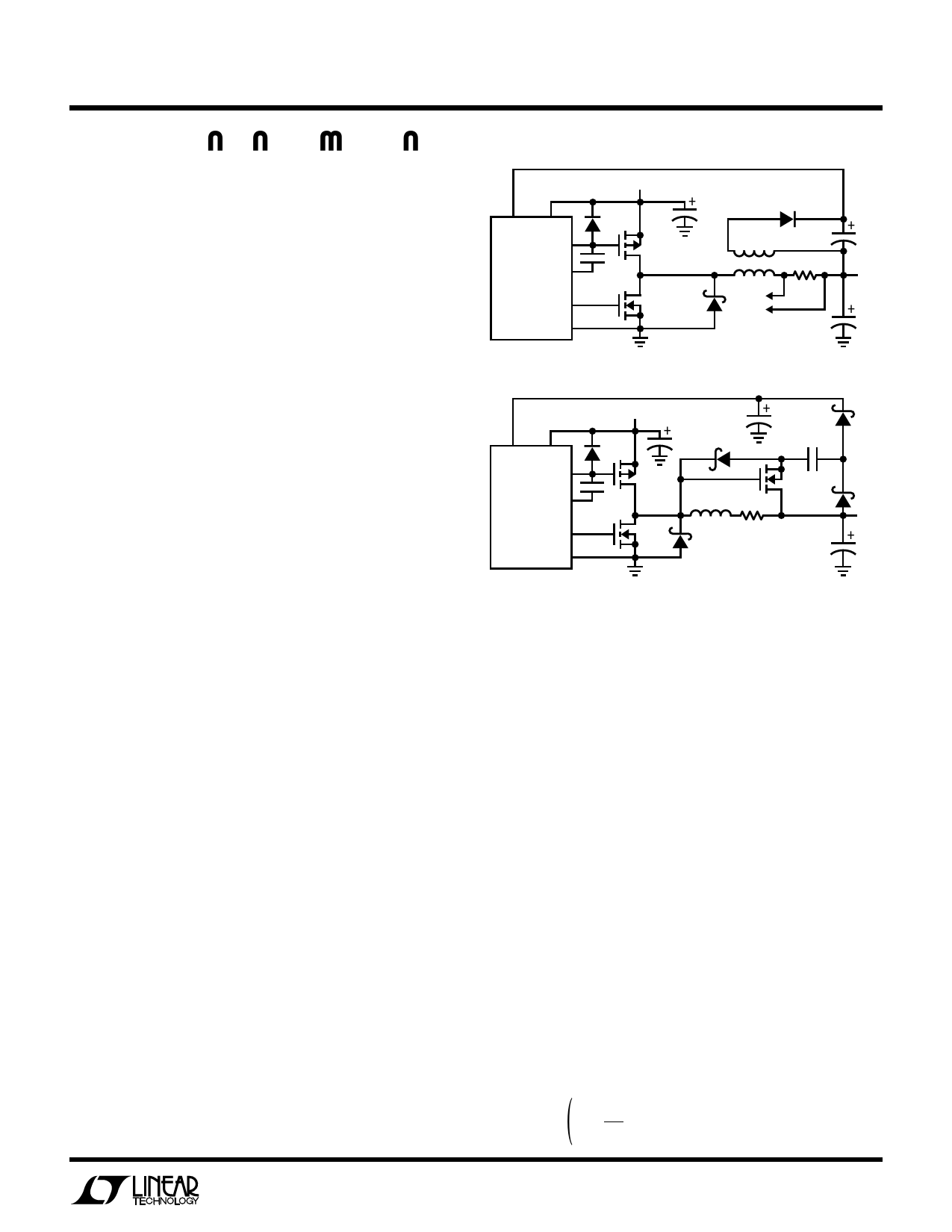
inductive boost winding shown in Figure 5a or the
capacitive charge pump shown in Figure 5b. The charge
pump has the advantage of simple magnetics and
generally provides the highest efficiency at the expense
of a slightly higher parts count.
LTC1267
LTC1267-ADJ/LTC1267-ADJ5
EXT VCC VIN
PGATE 3
PDRIVE 3
LTC1267
NGATE 3
VIN
P-CH
N-CH
1N4148
CIN
L
1:1 •
•
RSENSE
PGND3
LTC1267 • F05A
Figure 5a. Inductive Boost Circuit for EXT VCC
1µF
VOUT
3.3V
COUT
EXT VCC VIN
PGATE 3
PDRIVE 3
LTC1267
NGATE 3
PGND3
VIN
CIN BAT 85
1µF BAT 85
0.22µF
P-CH
VN2222LL
L RSENSE
BAT 85
N-CH
LTC1267 • F05B
Figure 5b. Capacitive Charge Pump for EXT VCC
VOUT
3.3V
COUT
4. EXT VCC connected to an external supply. If an external
supply is available in the 5V to 10V range it may be used
to power EXT VCC providing it is compatible with the
MOSFET gate drive requirements. When driving stan-
dard threshold MOSFETs, the external supply must
always be present during operation to prevent MOSFET
failure due to insufficient gate drive.
Under the condition that EXT VCC is connected to VOUT1
which is greater than 5.5V, to power down the whole
regulator, both the pins MSHDN and SHDN1 have to be
pulled high. If SHDN1 is left floating or grounded the
EXT VCC may self-power from VOUT1, preventing com-
plete shutdown.
LTC1267 Adjustable Applications
When an output voltage other than 3.3V or 5V is required,
the LTC1267-ADJ and LTC1267-ADJ5 adjustable ver-
sions are used with an external resistive divider from VOUT
to the VFB1, 2 pins. This is shown in Figure 6. The regulated
voltage is determined by:
) VOUT =
1 + R2
R1
1.25V
11
Share Link: 