LTC1153 Ver la hoja de datos (PDF) - Linear Technology
Número de pieza
componentes Descripción
Fabricante
LTC1153 Datasheet PDF : 16 Pages
| |||
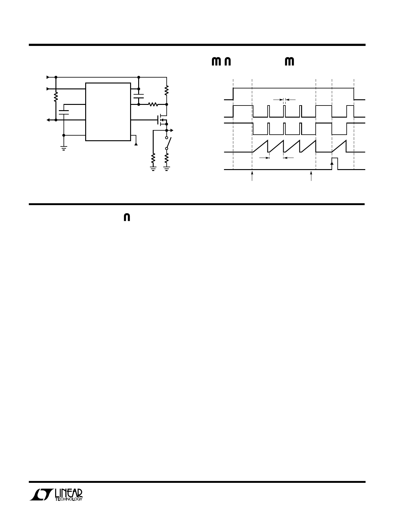
TEST CIRCUITS
WU
W
TI I G DIAGRA
LTC1153
5V
INPUT
STATUS
1 IN
51k
2
CT
0.1µF
LTC1153
Z5U 3
STATUS
8
VS
DS 7
6
G
CP
0.01µF
RSEN
0.05Ω
RD100k
IRLZ24
4
GND
5
SD
SHUTDOWN
OUTPUT
S1
10Ω 1Ω
LTC1153 • TC01
OFF NORMAL
INPUT
OUTPUT
OVER-CURRENT
(AUTO-CURRENT)
NOR- SHUT-
MAL DOWN OFF
*200µs
STATUS
TIMING
CAP
SHUT-
DOWN
*90ms
S1 CLOSED
S1 OPEN
*TIMES FOR COMPONENTS SHOWN IN TEST CIRCUIT
LTC1153 • TD01
U
LTC1153 OPERATIO
The LTC1153 is an electronic circuit breaker with built-in
MOSFET gate charge pump, over-current detection and
auto-reset circuitry. The LTC1153 consists of the follow-
ing functional blocks:
TTL and CMOS Compatible Inputs
The LTC1153 input and shutdown input have been de-
signed to accommodate a wide range of logic families.
Both input thresholds are set at about 1.3V with approxi-
mately 100mV of hysteresis.
A low standby current voltage regulator provides continu-
ous bias for the TTL-to-CMOS converter. The TTL-to-
CMOS converter output enables the rest of the circuitry. In
this way the power consumption is kept to a minimum in
the standby mode.
Internal Voltage Regulation
The output of the TTL-to-CMOS converter drives two
regulated supplies which power the low voltage CMOS
logic and analog blocks. The regulator outputs are isolated
from each other so that the noise generated by the charge
pump logic is not coupled into the 100mV reference or the
analog comparator.
Gate Charge Pump
Gate drive for the MOSFET switch is produced by an
adaptive charge pump circuit which generates a gate
voltage substantially higher than the power supply volt-
age. The charge pump capacitors are included on-chip and
therefore no external components are required to generate
the gate drive.
Auto-Reset Timer
An external timing capacitor, CT, is ramped up by a small
current whenever a fault is detected, i.e., the switch
latched off. When the timing capacitor ramps up to ap-
proximately 2.5V, the switch is turned back on and the
timing capacitor discharged. If the circuit breaker output
is still in an overload state, the breaker will latch off and this
cycle will continue until the fault condition is removed.
Drain Current Sense
The LTC1153 is configured to sense the current flowing
into the drain of an N-channel MOSFET switch. An internal
100mV reference is compared to the drop across a sense
resistor (typically 0.002Ω to 0.10Ω) in series with the
drain lead. If the drop across this resistor exceeds the
internal 100mV threshold, the input latch is reset and the
gate is quickly discharged via a relatively large N-channel
transistor.
7
Share Link: 