LT5528EUF Ver la hoja de datos (PDF) - Linear Technology
Número de pieza
componentes Descripción
Fabricante
LT5528EUF Datasheet PDF : 16 Pages
| |||
LT5528
APPLICATIO S I FOR ATIO
and 12pF to ground is incorporated (see Figure 1), which
limits the baseband bandwidth to approximately 330MHz
(–1dB point). The common-mode voltage is about 0.52V
and is approximately constant over temperature.
It is important that the applied common-mode voltage level
of the I and Q inputs is about 0.52V in order to properly
bias the LT5528. Some I/Q test generators allow setting
the common-mode voltage independently. In this case, the
common-mode voltage of those generators must be set
to 0.26V to match the LT5528 internal bias, because for
DC signals, there is no –6dB source-load voltage division
(see Figure 2).
50Ω
–+ 0.52VDC
GENERATOR
0.26VDC
50Ω
50Ω
45Ω
–+ 0.52VDC
GENERATOR
0.52VDC
0.52VDC –+
LT5528
5528 F02
Figure 2. DC Voltage Levels for a Generator Programmed at
0.26VDC for a 50Ω Load and the LT5528 as a Load
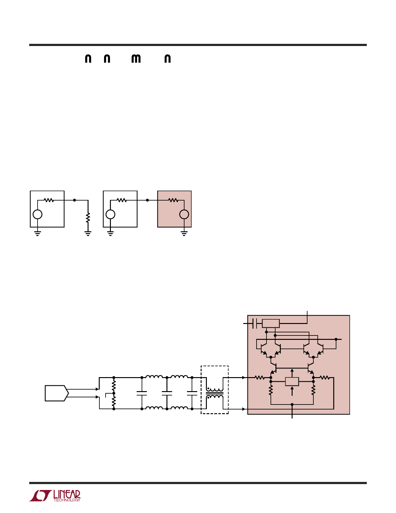
It is recommended that the part be driven differentially;
otherwise, the even-order distortion products will de-
grade the overall linearity severely. Typically, a DAC will
be the signal source for the LT5528. To prevent aliasing,
a filter should be placed between the DAC output and the
LT5528’s baseband inputs. In Figure 3, an example interface
schematic shows a commonly used DAC output interface
followed by a passive 5th order ladder filter. The DAC in
this example sources a current from 0mA to 20mA. The
interface may be DC coupled. This allows adjustment of
the DAC’s differential output current to minimize the LO
feed-through. Optionally, transformer T1 can be inserted
to improve the current balance in the BBPI and BBMI pins.
This will improve the second-order distortion performance
(OIP2).
The maximum single sideband CW RF output power at
2GHz using 20mA drive to both I and Q channels with the
configuration shown in Figure 3 is about –2.5dBm. The
maximum CW output power can be increased by con-
necting resistors R5 and R6 to –5V instead of GND, and
changing their values to 550Ω. In that case, the maximum
single sideband CW RF output power at 2GHz will be about
2.3dBm. In addition, the ladder filter component values
require adjustment for a higher source impedance.
VCC = 5V
RF = –2.5dBm, MAX
BALUN
C
LOMI
LT5528
LOPI
0.5V
0mA TO 20mA
R5, 50Ω
DAC
C1
0mA TO 20mA GND R6, 50Ω
L1A
C2
L1B
L2A
C3
L2B
OPTIONAL
BBPI
T1
1:1
BBMI
R1
45Ω
CM
R3
VREF = 0.52V
R2
45Ω
R4
0.5V
GND
5528 F03
Figure 3. LT5528 5th Order Filtered Baseband Interface with Common DAC (Only I-Channel is Shown)
5528f
9
Share Link: 