LT5528EUF Ver la hoja de datos (PDF) - Linear Technology
Número de pieza
componentes Descripción
Fabricante
LT5528EUF Datasheet PDF : 16 Pages
| |||
FEATURES
■ Direct Conversion to 1.5GHz to 2.4GHz
■ High OIP3: 21.8dBm at 2GHz
■ Low Output Noise Floor at 5MHz Offset:
No RF: –159.3dBm/Hz
POUT = 4dBm: –151.8dBm/Hz
■ 4-Ch W-CDMA ACPR: –66dBc at 2.14GHz
■ Integrated LO Buffer and LO Quadrature Phase
Generator
■ 50Ω AC-Coupled Single-Ended LO and RF Ports
■ 50Ω DC Interface to Baseband Inputs
■ Low Carrier Leakage: –42dBm at 2GHz
■ High Image Rejection: 45dB at 2GHz
■ 16-Lead QFN 4mm × 4mm Package
U
APPLICATIO S
■ Infrastructure Tx for DCS, PCS and UMTS Bands
■ Image Reject Up-Converters for PCS and UMTS
Bands
■ Low-Noise Variable Phase-Shifter for 1.5GHz to
2.4GHz Local Oscillator Signals
LT5528
1.5GHz to 2.4GHz
High Linearity Direct
Quadrature Modulator
DESCRIPTIO
The LT®5528 is a direct I/Q modulator designed for high
performance wireless applications, including wireless
infrastructure. It allows direct modulation of an RF signal
using differential baseband I and Q signals. It supports
PHS, GSM, EDGE, TD-SCDMA, CDMA, CDMA2000,
W-CDMA and other systems. It may also be configured
as an image reject up-converting mixer, by applying
90° phase-shifted signals to the I and Q inputs. The I/Q
baseband inputs consist of voltage-to-current converters
that in turn drive double-balanced mixers. The outputs of
these mixers are summed and applied to an on-chip RF
transformer, which converts the differential mixer signals
to a 50Ω single-ended output. The four balanced I and Q
baseband input ports are intended for DC coupling from a
source with a common-mode voltage level of about 0.5V.
The LO path consists of an LO buffer with single-ended
input, and precision quadrature generators that produce
the LO drive for the mixers. The supply voltage range is
4.5V to 5.25V.
, LTC and LT are registered trademarks of Linear Technology Corporation.
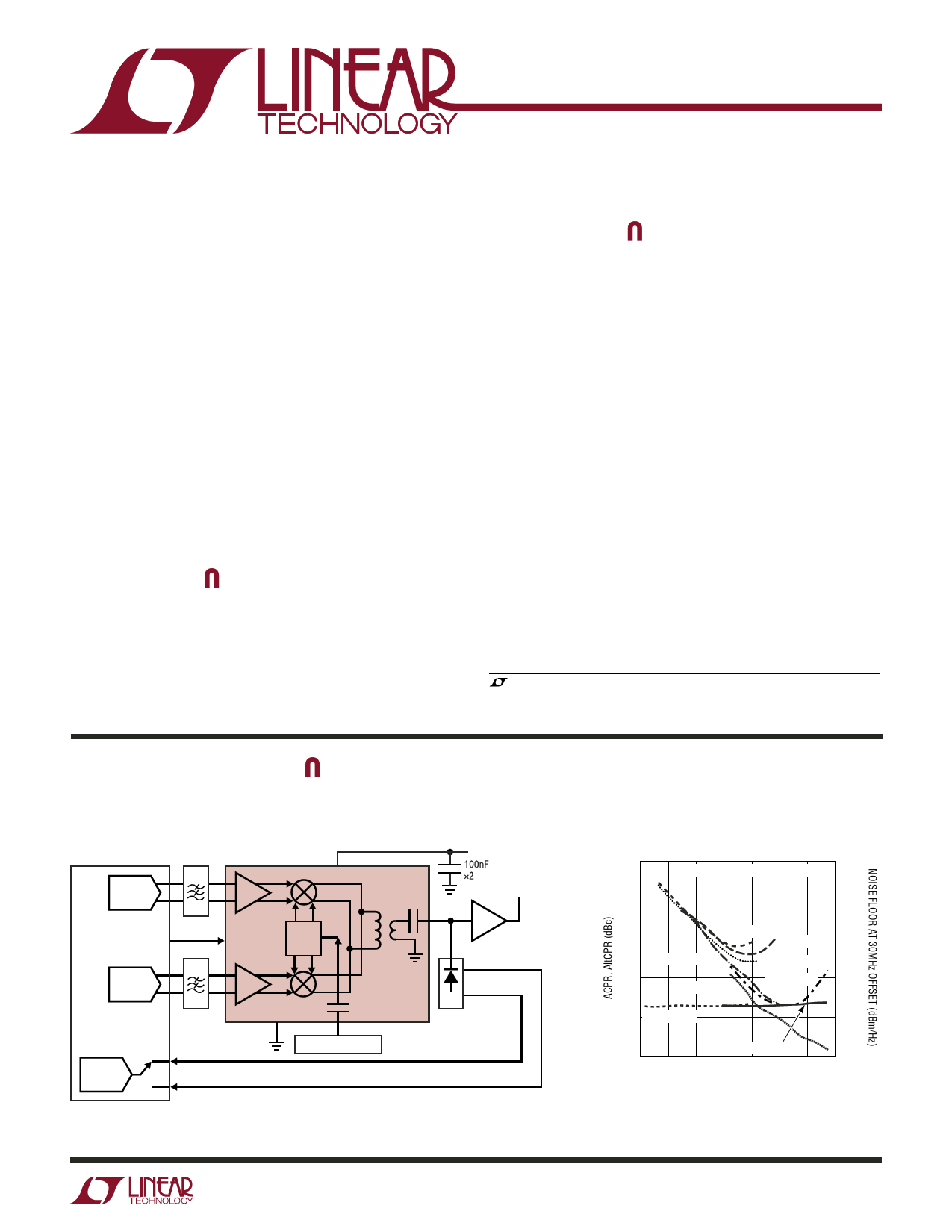
TYPICAL APPLICATIO
1.5GHz to 2.4GHz Direct Conversion Transmitter Application
with LO Feed-Through and Image Calibration Loop
I-DAC
14
16 V-I
VCC 8, 13
LT5528
5V
RF = 1.5GHz
TO 2.4GHz
W-CDMA ACPR, AltCPR and Noise vs RF Output
Power at 2140MHz for 1, 2 and 4 Channels
–55
–140
DOWNLINK TEST MODEL 64 DPCH
–60
–145
EN
Q-DAC
I-CHANNEL
1
0°
90°
7 Q-CHANNEL
5 V-I
11
PA
4-CH ACPR
–65
2-CH ACPR –150
BALUN
LO FEED-THROUGH CAL OUT
2-CH AltCPR
4-CH AltCPR
IMAGE CAL OUT
–70
1-CH ACPR
–155
1-CH AltCPR
CAL
BASEBAND
DSP
ADC
2, 4, 6, 9, 10, 12, 15, 17
3
VCO/SYNTHESIZER
–75 4-CH NOISE
–160
1-CH NOISE
–80
–165
–42 –38 –34 –30 –26 –22 –18 –14
RF OUTPUT POWER PER CARRIER (dBm)
5528 TA01a
5528 TA01b
5528f
1
Share Link: 