LT5524EFE Ver la hoja de datos (PDF) - Linear Technology
Número de pieza
componentes Descripción
Fabricante
LT5524EFE Datasheet PDF : 16 Pages
| |||
LT5524
APPLICATIO S I FOR ATIO
Clipping Free Operation
The LT5524 is a class A amplifier. To avoid signal distor-
tion, the user must ensure that the LT5524 outputs do not
enter into current or voltage limiting. The following discus-
sion applies to maximum gain operation.
To avoid current clipping, the output signal current should
not exceed the DC quiescent current, IOUT = 20mA (typi-
cal). Correspondingly, the maximum input voltage,
VIN(MAX), is IOUT/gm = 133mV (peak). In power terms,
PIN(MAX) = –11.5dBm (assuming RIN = 122Ω).
To avoid output voltage clipping (due to LT5524 output
stage saturation or breakdown), the single-ended output
voltage swing should stay within the specified limits; i.e.,
2V ≤ VOUT ≤ 8V. For a DC output bias of 5V, the maximum
single ended swing will be 3Vpeak and the maximum
differential swing will be 6Vpeak. The simultaneous onset
of both current and voltage limiting occurs when ROUT =
6Vpeak/20mA = 300Ω (typ) for a maximum POUT =
17.8dBm. This calculation applies for a sinusoidal signal.
For nonsinusoidal signals, use the appropriate crest fac-
tor to calculate the actual maximum power that avoids
output clipping.
Although the instantaneous AC voltage on the OUT+ or
OUT– pins may in some situations safely exceed 8V (with
respect to ground), in no case should the DC voltage on
these pins be allowed to exceed the ABSMAX tested limit
of 7V.
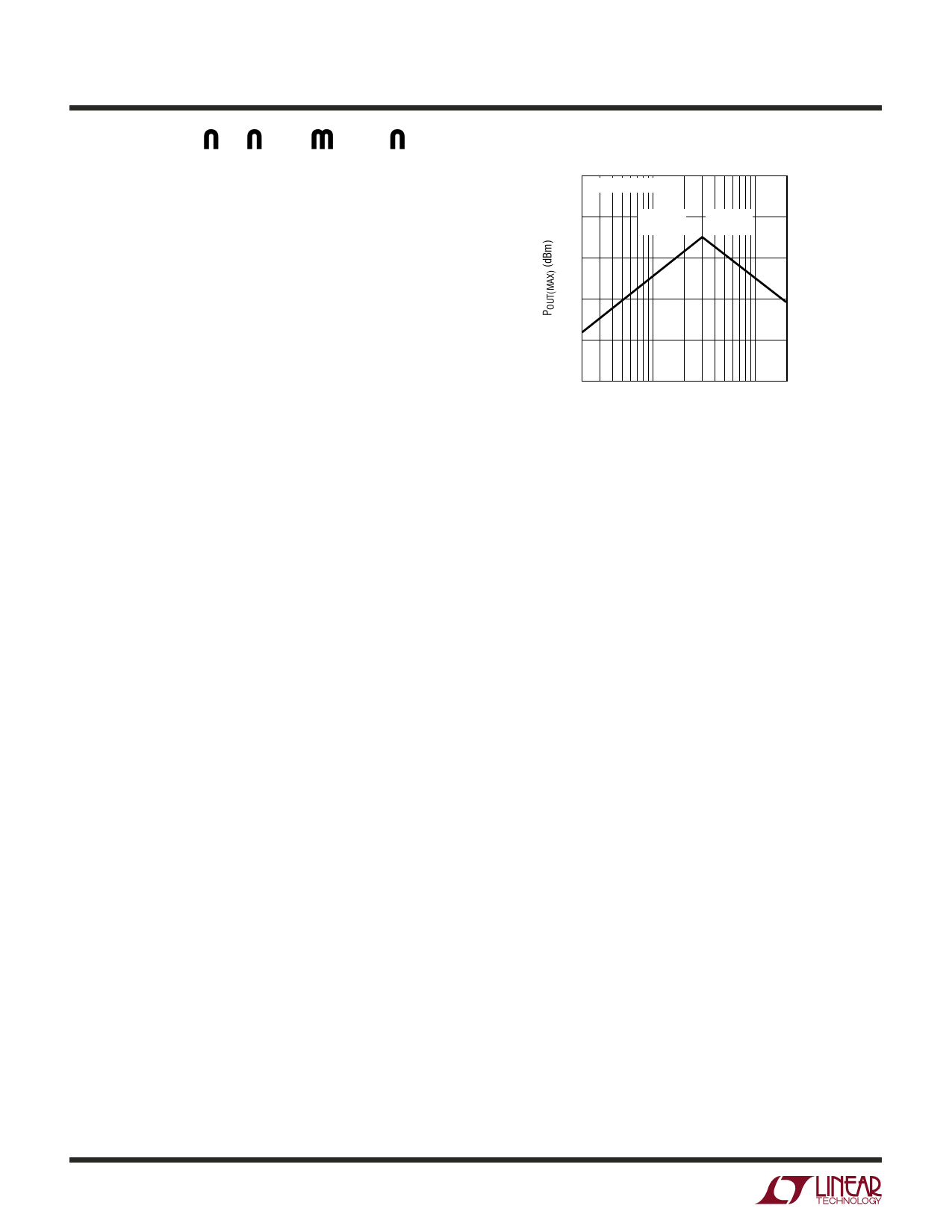
For nonoptimal ROUT values, the maximum available out-
put power will be lower and can be calculated (considering
current limiting for ROUT < 300Ω, and voltage limiting for
ROUT > 300Ω). The result of this calculation is shown in
Figure 7.
The LT5524 input should not be overdriven (PIN >
–11.5dBm at maximum gain). The consequences of over-
drive are reduced bandwidth and, when the frequency is
greater than 50MHz, reduced output power. At reduced
gain settings, the maximum PIN is increased by an amount
equal to the gain reduction.
Input Bias Voltage
The LT5524 IN+, IN– signal inputs are internally biased to
1.48V common mode when enabled, and to 1.26V in
10
25
VCC = VCCO = 5V
20
CURRENT
LIMIT
15
VOLTAGE
LIMIT
10
5
0
20
100
1000 2000
ROUT (Ω)
5524 F07
Figure 7. Maximum Output Power as a Function of ROUT
shutdown mode. These inputs are typically coupled by
means of a capacitor or a transformer to a signal source,
and impedance matching is assumed. In shutdown mode,
the internal bias can handle up to 1µA leakage on the input
coupling capacitors. This reduces the turn-on delay due to
the input coupling RC time constant when exiting shut-
down mode.
If DC coupling to the input is required, the external
common mode bias should track the LT5524’s internal
common mode level. The DC current from the LT5524
inputs should not exceed IIN(SINK) = –200µA and IIN(SOURCE)
= 400µA.
Stability Considerations
The LT5524’s open-loop architecture allows it to drive any
practical load. Note that LT5524 gain is proportional to the
load impedance, and may exceed the reverse isolation at
frequencies above 1GHz if the LT5524’s outputs are left
unloaded, with instability as the undesirable consequence.
In such cases, placing a resistive differential load (e.g., 4k)
or a small capacitor at the LT5524 outputs can be used to
limit the maximum gain.
The LT5524 has about 20GHz gain-bandwidth product.
Hence, attention must be paid to the printed circuit board
layout to avoid output pin to input pin signal coupling (the
evaluation board layout is a good example). Due to the
LT5524’s internal power supply regulator, external supply
decoupling capacitors typically are not required. Likewise,
decoupling capacitors on the LT5524 control inputs typi-
cally are not needed. Note, however, that the Exposed Pad
5524f
Share Link: 