LT3957AIUHE Ver la hoja de datos (PDF) - Linear Technology
Número de pieza
componentes Descripción
Fabricante
LT3957AIUHE Datasheet PDF : 28 Pages
| |||
LT3957A
ELECTRICAL CHARACTERISTICS The l denotes the specifications which apply over the full operating temp-
erature range, otherwise specifications are at TA ≈ TJ = 25°C. VIN = 24V, EN/UVLO = 24V, SENSE2 = 0V, unless otherwise noted.
PARAMETER
CONDITIONS
MIN TYP MAX UNITS
INTVCC Current Limit
INTVCC Load Regulation (ΔVINTVCC / VINTVCC)
INTVCC Line Regulation (ΔVINTVCC / [ΔVIN • VINTVCC])
Dropout Voltage (VIN – VINTVCC)
INTVCC Current in Shutdown
INTVCC Voltage to Bypass Internal LDO
Logic Inputs
VIN = 40V
VIN = 15V
0 < IINTVCC < 20mA, VIN = 8V
6V < VIN < 40V
VIN = 5V, IINTVCC = 20mA, VC = 0V
EN/UVLO = 0V, INTVCC = 6V
32
40
55
mA
95
mA
–1
–0.5
%
0.02 0.05
%/ V
450
mV
17
μA
5.5
V
EN/UVLO Threshold Voltage Falling
EN/UVLO Voltage Hysteresis
VIN = INTVCC = 6V
l 1.17 1.22 1.27
V
20
mV
EN/UVLO Input Low Voltage
EN/UVLO Pin Bias Current Low
IVIN Drops Below 1μA
EN/UVLO = 1.15V
0.4
V
1.7
2
2.5
μA
EN/UVLO Pin Bias Current High
EN/UVLO = 1.33V
20
100
nA
Note 1: Stresses beyond those listed under Absolute Maximum Ratings
may cause permanent damage to the device. Exposure to any Absolute
Maximum Rating condition for extended periods may affect device
reliability and lifetime.
Note 2: The LT3957AE is guaranteed to meet performance specifications
from the 0°C to 125°C operating junction temperature. Specifications over
the –40°C to 125°C operating junction temperature range are assured by
design, characterization and correlation with statistical process controls.
The LT3957AI is guaranteed over the full –40°C to 125°C operating
junction temperature range.
Note 3: The LT3957A is tested in a feedback loop which servos VFBX to the
reference voltages (1.6V and –0.8V) with the VC pin forced to 1.3V.
Note 4: FBX overvoltage lockout is measured at VFBX(OVERVOLTAGE) relative
to regulated VFBX(REG).
Note 5: For 3V ≤ VIN < 6V, the EN/UVLO pin must not exceed VIN.
Note 6: EN/UVLO = 1.33V when VIN = 3V.
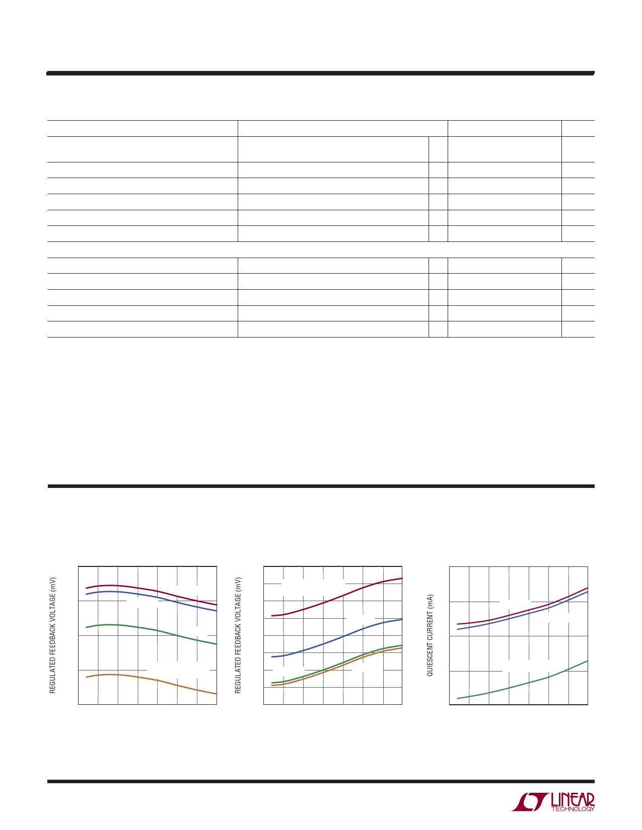
TYPICAL PERFORMANCE CHARACTERISTICS TA ≈ TJ = 25°C, unless otherwise noted.
Positive Feedback Voltage
vs Temperature, VIN
1605
1600
VIN = 24V
VIN = 40V
1590
VIN = 8V
1585
VIN = INTVCC = 3V,
SHDN/UVLO = 1.33V
1580
–50 –25
0 25 50 75
TEMPERATURE (°C)
100 125
3957A G01
Negative Feedback Voltage
vs Temperature, VIN
–788
–790
–792
VIN = INTVCC = 3V
SHDN/UVLO = 1.33V
–794
–796
VIN = 8V
–798
–800
–802
VIN = 24V
VIN = 40V
–804
–50 –25
0 25 50 75
TEMPERATURE (°C)
100 125
3957A G02
Quiescent Current
vs Temperature, VIN
1.8
1.7
VIN = 40V
VIN = 24V
1.6
1.5
VIN = INTVCC = 3V
1.4
–50 –25
0 25 50 75
TEMPERATURE (°C)
100 125
3957A G03
3957afa
4
Share Link: 