LT3957AIUHE Ver la hoja de datos (PDF) - Linear Technology
Número de pieza
componentes Descripción
Fabricante
LT3957AIUHE Datasheet PDF : 28 Pages
| |||
LT3957A
APPLICATIONS INFORMATION
undervoltage (UV) threshold is 2.7V (typical), with 0.1V
hysteresis, to ensure that the internal MOSFET has suf-
ficient gate drive voltage before turning on. When INTVCC
is below the UV threshold, the internal power switch will
be turned off and the soft-start operation will be triggered.
The logic circuitry within the LT3957A is also powered
from the internal INTVCC supply.
The INTVCC regulator must be bypassed to SGND imme-
diately adjacent to the IC pins with a minimum of 4.7μF
ceramic capacitor. Good bypassing is necessary to sup-
ply the high transient currents required by the MOSFET
gate driver.
In an actual application, most of the IC supply current is
used to drive the gate capacitance of the internal power
MOSFET. The on-chip power dissipation can be significant
when the internal power MOSFET is being driven at a high
frequency and the VIN voltage is high.
An effective approach to reduce the power consumption of
the internal LDO for gate drive and to improve the efficiency
is to tie the INTVCC pin to an external voltage source high
enough to turn off the internal LDO regulator.
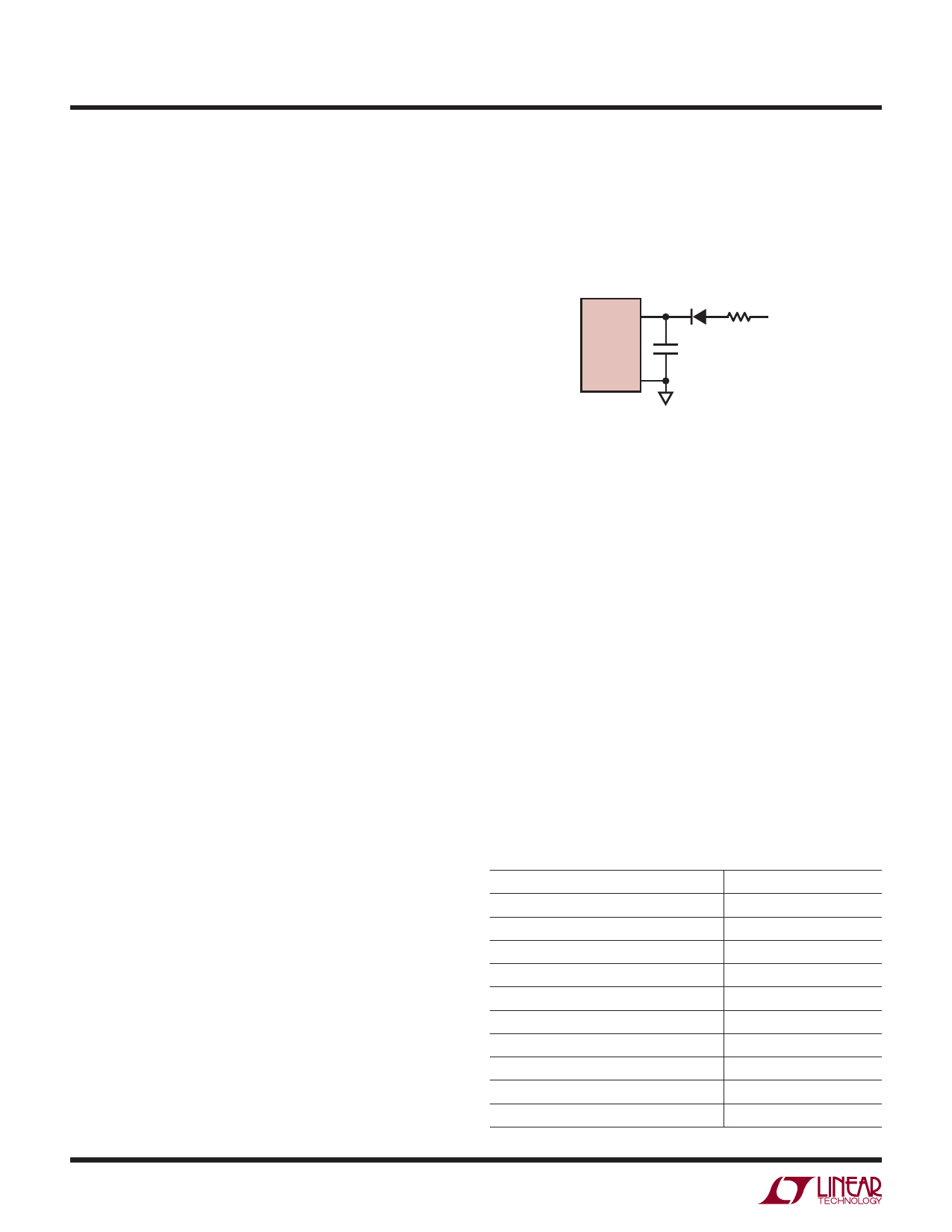
In SEPIC or flyback applications, the INTVCC pin can be
connected to the output voltage VOUT through a blocking
diode, as shown in Figure 2, if VOUT meets the following
conditions:
1. VOUT < VIN (pin voltage)
2. VOUT < 8V
A resistor RVCC can be connected, as shown in Figure 2, to
limit the inrush current from VOUT. Regardless of whether
or not the INTVCC pin is connected to an external voltage
source, it is always necessary to have the driver circuitry
bypassed with a 4.7μF low ESR ceramic capacitor to ground
immediately adjacent to the INTVCC and SGND pins.
If LT3957A operates at a low VIN and high switching fre-
quency, the voltage drop across the drain and the source
of the LDO PMOS (M2 in Figure 1) could push INTVCC to
be below the UV threshold. To prevent this from happening,
the INTVCC pin can be shorted directly to the VIN pin. VIN
must not exceed the INTVCC Absolute Maximum Rating
(8V). In this condition, the internal LDO will be turned off
and the gate driver will be powered directly from VIN. It is
10
recommended that INTVCC pin be shorted to the VIN pin if
VIN is lower than 3.5V at 1MHz switching frequency, or VIN
is lower than 3.2V at 100kHz switching frequency. With
the INTVCC pin shorted to VIN, however, a small current
(around 16μA) will load the INTVCC in shutdown mode.
INTVCC
LT3957A
SGND
DVCC RVCC
CVCC
4.7μF
VOUT
3957A F02
Figure 2. Connecting INTVCC to VOUT
Operating Frequency and Synchronization
The choice of operating frequency may be determined
by on-chip power dissipation (a low switching frequency
may be required to ensure IC junction temperature does
not exceed 125°C), otherwise it is a trade-off between
efficiency and component size. Low frequency operation
improves efficiency by reducing gate drive current and
MOSFET and diode switching losses. However, lower
frequency operation requires a physically larger induc-
tor. Switching frequency also has implications for loop
compensation. The LT3957A uses a constant-frequency
architecture that can be programmed over a 100kHz to
1000kHz range with a single external resistor from the RT
pin to SGND, as shown in Figure 1. A table for selecting
the value of RT for a given operating frequency is shown
in Table 1.
Table 1. Timing Resistor (RT) Value
SWITCHING FREQUENCY (kHz)
100
200
300
400
500
600
700
800
900
1000
RT (kΩ)
140
63.4
41.2
30.9
24.3
19.6
16.5
14
12.1
10.5
3957afa
Share Link: 