LT3580EDD-TRPBF Ver la hoja de datos (PDF) - Linear Technology
Número de pieza
componentes Descripción
Fabricante
LT3580EDD-TRPBF
Linear Technology

LT3580EDD-TRPBF Datasheet PDF : 28 Pages
| |||
LT3580
BLOCK DIAGRAM
RC
CSS
CC
VIN
CIN
SHDN
7
SS
2
VC
5
–
1.3V +
DISCHARGE
DETECT
L1
UVLO
VIN
3
1.215V
REFERENCE
SR2
R
Q
S
275k
SOFT-
START
Q2
VC
ILIMIT
SW
D1
4
COMPARATOR
–
SR1
DRIVER
C1
A3
R
Q
Q1
+
S
+
14.6k
A1
∑
A4
0.01Ω
–
FB
1
+
14.6k
A2
RAMP
GENERATOR
FREQUENCY ÷N ADJUSTABLE
FOLDBACK
OSCILLATOR
GND
9
–
SYNC
BLOCK
SYNC
8
RT
6
RT
VOUT
RFB
3580 BD
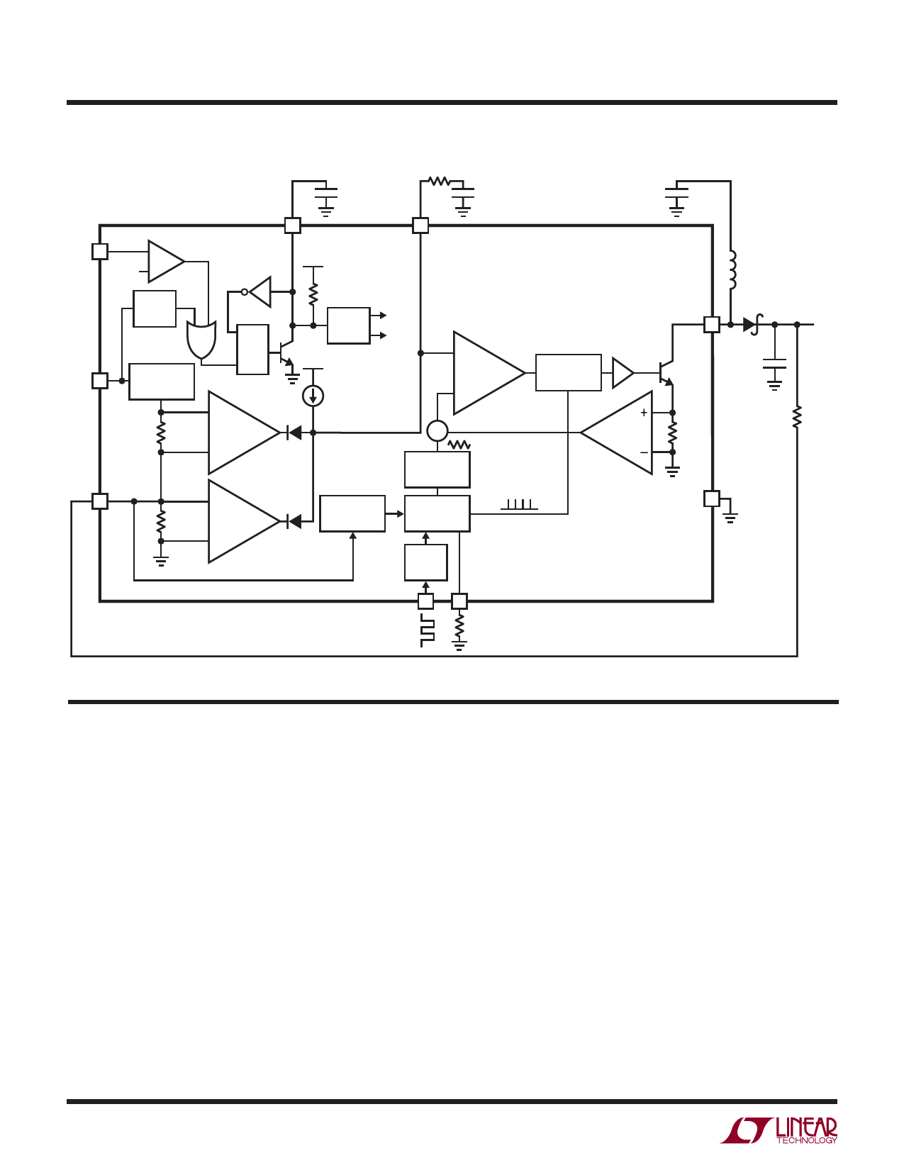
OPERATION
The LT3580 uses a constant-frequency, current mode con-
trol scheme to provide excellent line and load regulation.
Refer to the Block Diagram which shows the LT3580 in a
boost configuration. At the start of each oscillator cycle,
the SR latch (SR1) is set, which turns on the power switch,
Q1. The switch current flows through the internal current
sense resistor generating a voltage proportional to the
switch current. This voltage (amplified by A4) is added
to a stabilizing ramp and the resulting sum is fed into the
positive terminal of the PWM comparator A3. When this
voltage exceeds the level at the negative input of A3, the SR
latch is reset, turning off the power switch. The level at the
negative input of A3 (VC pin) is set by the error amplifier A1
(or A2) and is simply an amplified version of the difference
between the feedback voltage (FB pin) and the reference
voltage (1.215V or 5mV depending on the configuration).
In this manner, the error amplifier sets the correct peak
current level to keep the output in regulation.
The LT3580 has a novel FB pin architecture that can be
used for either boost or inverting configurations. When
configured as a boost converter, the FB pin is pulled up
to the internal bias voltage of 1.215V by the RFB resistor
connected from VOUT to FB. Comparator A2 becomes
inactive and comparator A1 performs the inverting
amplification from FB to VC. When the LT3580 is in an
inverting configuration, the FB pin is pulled down to 5mV
by the RFB resistor connected from VOUT to FB. Comparator
A1 becomes inactive and comparator A2 performs the
noninverting amplification from FB to VC.
3580fg
6
Share Link: