LT3580EDD-TRPBF Ver la hoja de datos (PDF) - Linear Technology
Número de pieza
componentes Descripción
Fabricante
LT3580EDD-TRPBF
Linear Technology

LT3580EDD-TRPBF Datasheet PDF : 28 Pages
| |||
LT3580
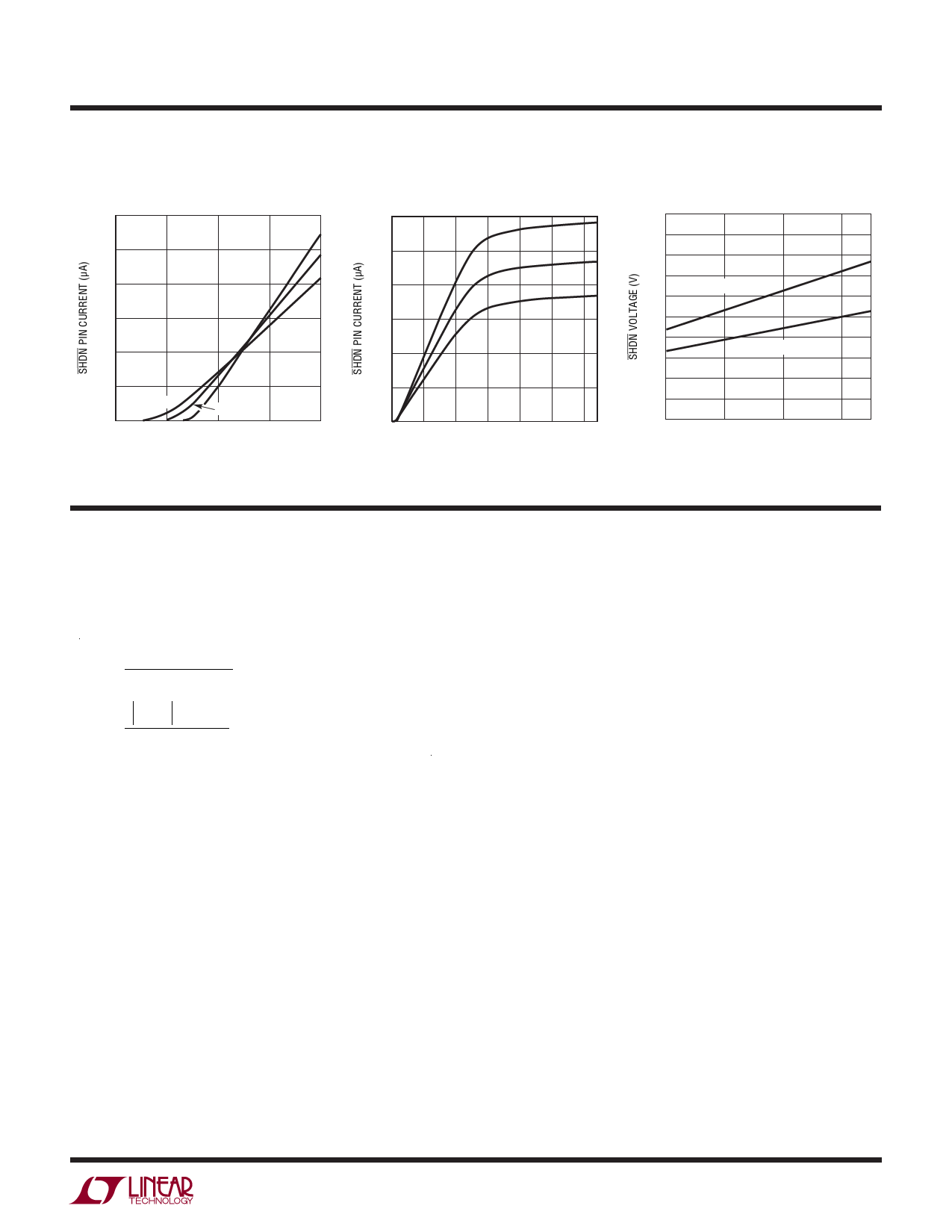
TYPICAL PERFORMANCE CHARACTERISTICS TA = 25°C unless otherwise specified
SHDN Pin Current
30
25
20
15
10
5
0
0
–50°C
100°C
20°C
0.5
1
1.5
SHDN VOLTAGE (V)
2
3580 G10
SHDN Pin Current
300
–50°C
250
20°C
200
100°C
150
100
50
0
0 5 10 15 20 25 30
SHDN VOLTAGE (V)
3580 G11
Active/Lockout Threshold
1.40
1.38
1.36
1.34
SHDN RISING
1.32
1.30
1.28
SHDN FALLING
1.26
1.24
1.22
1.20
–50
0
50
TEMPERATURE (°C)
100
3580 G12
PIN FUNCTIONS
FB (Pin 1): Positive and Negative Feedback Pin. For a
boost or inverting converter, tie a resistor from the FB pin
to VOUT according to the following equations:
( ) RFB =
VOUT − 1.215
83.3 • 10−6
; Boost or SEPIC Converter
( ) RFB =
VOUT + 5mV
83.3 • 10−6
;
Inverting Converter
VC (Pin 2): Error Amplifier Output Pin. Tie external
compensation network to this pin.
VIN (Pin 3): Input Supply Pin. Must be locally bypassed.
SW (Pin 4): Switch Pin. This is the collector of the internal
NPN Power switch. Minimize the metal trace area connec-
ted to this pin to minimize EMI.
SHDN (Pin 5): Shutdown Pin. In conjunction with the
UVLO (undervoltage lockout) circuit, this pin is used
to enable/disable the chip and restart the soft-start
sequence. Drive below 1.24V (LT3580E, LT3580I) or 1.22V
(LT3580H, LT3580MP) to disable the chip. Drive above
1.38V (LT3580E, LT3580I) or 1.40V (LT3580H, LT3580MP)
to activate chip and restart the soft-start sequence. Do
not float this pin.
RT (Pin 6): Timing Resistor Pin. Adjusts the switching
frequency. Place a resistor from this pin to ground to set
the frequency to a fixed free running level. Do not float
this pin.
SS (Pin 7): Soft-Start Pin. Place a soft-start capacitor here.
Upon start-up, the SS pin will be charged by a (nominally)
275k resistor to about 2.2V.
SYNC (Pin 8): To synchronize the switching frequency to
an outside clock, simply drive this pin with a clock. The
high voltage level of the clock needs to exceed 1.3V, and
the low level should be less 0.4V. Drive this pin to less than
0.4V to revert to the internal free running clock. See the
Applications Information section for more information.
GND (Exposed Pad Pin 9): Ground. Exposed pad must
be soldered directly to local ground plane.
3580fg
5
Share Link: