LT3500 Ver la hoja de datos (PDF) - Linear Technology
Número de pieza
componentes Descripción
Fabricante
LT3500 Datasheet PDF : 28 Pages
| |||
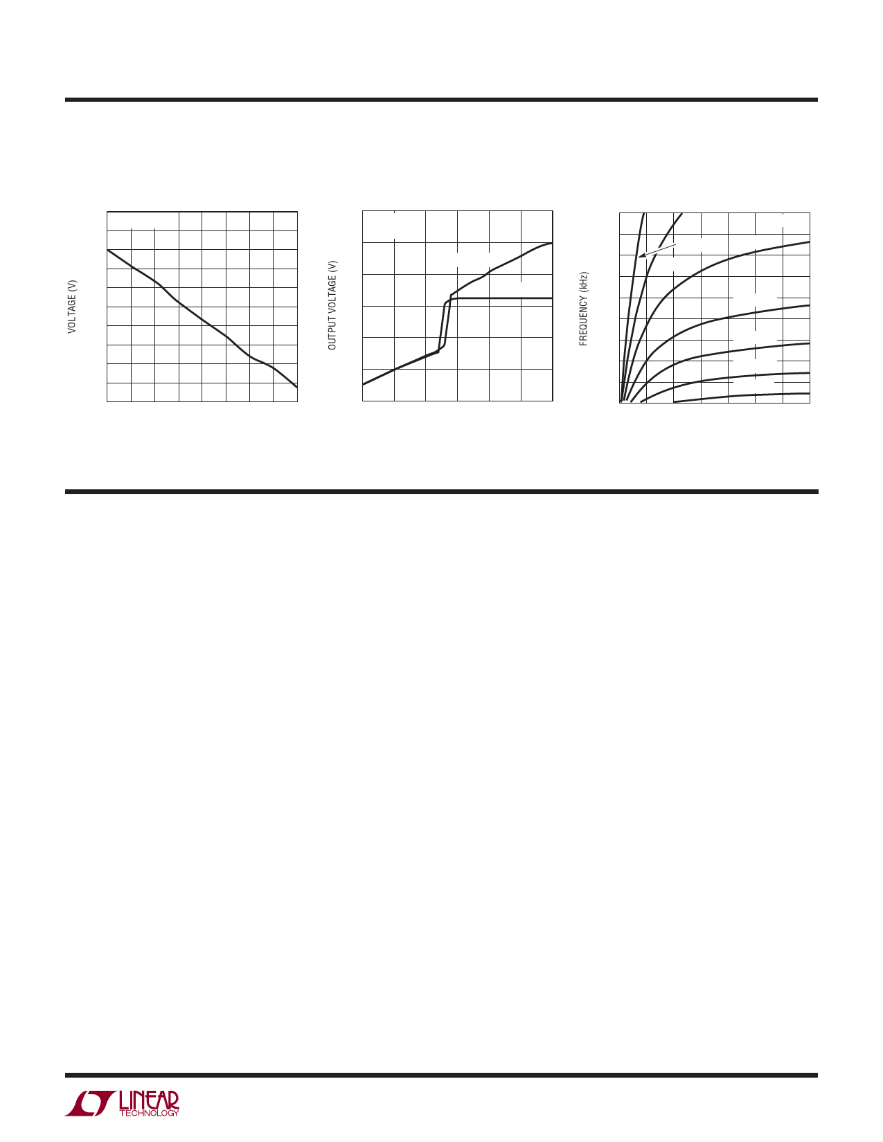
TYPICAL PERFORMANCE CHARACTERISTICS
LDRV Dropout Voltage
vs Temperature
1.50
ILDRV = 5mA
1.45
1.40
1.35
1.30
1.25
1.20
1.15
1.10
1.05
1.00
–50 –25 0 25 50 75 100 125 150
TEMPERATURE (°C)
3500 G22
Switcher Dropout Operation
6
IVOUT1 = 1A
TA = 25°C
5
VVOUT1 = 5V
4
VVOUT1 = 3.3V
3
2
1
0
2.5 3.0 3.5 4.0 4.5 5.0 5.5
INPUT VOLTAGE (V)
3500 G23
LT3500
Inductor Value for 2A Maximum
Load Current (VOUT1 = 3.3V,
IRIPPLE = 250mA)
2500
2250
2000
1750
L = 1μH
L = 1.5μH
TA = 25°C
L = 2.2μH
1500
1250
1000
L = 3.3μH
L = 4.7μH
750
500
250
5
L = 6.8μH
L = 10μH
10 15 20 25 30 35 40
INPUT VOLTAGE (V)
3500 G24
PIN FUNCTIONS
VIN: The VIN pin powers the internal control circuitry and
is monitored by an undervoltage comparator. The VIN pin
is also connected to the collectors of the internal power
NPN switch and linear output NPN. The VIN pin has high
dI/dt edges and must be decoupled to ground close to
the pin of the device.
SHDN: The SHDN pin is used to shut down the LT3500
and reduce quiescent current to a typical value of
12μA. The accurate 0.76V threshold and input current
hysteresis can be used as an undervoltage lockout, prevent-
ing the regulator from operating until the input voltage has
reached a predetermined level. Force the SHDN pin above
its threshold or let it float for normal operation.
SS: The SS pin is used to control the slew rate of the
output of both the switching and linear regulators. A
single capacitor from the SS pin to ground determines
the regulators’ ramp rate. For soft-start details see the
Applications Information section.
PG: The power good pin is an open-collector output that
sinks current when the FB or LFB falls below 90% of its
nominal regulating voltage. For VIN above 2V, its output
state remains true, although during SHDN, VIN undervoltage
lockout, or thermal shutdown, its current sink capability
is reduced
VC: The VC pin is the output of the error amplifier and the
input to the peak switch current comparator. It is normally
used for frequency compensation, but can also be used
as a current clamp or control loop override. If the error
amplifier drives VC above the maximum switch current
level, a voltage clamp activates. This indicates that the
output is overloaded and current to be pulled from the
SS pin reducing the regulation point.
RT/SYNC: This RT/SYNC pin provides two modes of setting
the constant switch frequency.
Connecting a resistor from the RT/SYNC pin to ground
will set the RT/SYNC pin to a typical value of 1V. The
resultant switching frequency will be set by the resistor
value. The minimum value of 15kΩ and maximum value
of 200kΩ set the switching frequency to 2.5MHz and
250kHz respectively.
3500fc
7
Share Link: 