LT3489 Ver la hoja de datos (PDF) - Linear Technology
Número de pieza
componentes Descripción
Fabricante
LT3489 Datasheet PDF : 12 Pages
| |||
LT3489
APPLICATIO S I FOR ATIO
Diode Selection
Schottky diodes, with their low forward voltage drop and
fast switching speed, are ideal for LT3489 applications.
Table 3 lists several Schottky diodes that work well with the
LT3489. The diode’s average current rating must exceed
the average output current. The diode’s maximum reverse
voltage must exceed the output voltage. The diode conducts
current only when the power switch is turned off (typically
less than 50% duty cycle), so a 3A diode is sufficient for
most designs. The companies below also offer Schottky
diodes with high voltage and current ratings.
Table 3. Suggested Diodes
MAXIMUM
MANUFACTURER MAXIMUM REVERSE
PART NUMBER CURRENT (A) VOLTAGE (V)
MANUFACTURER
UPS340
UPS315
3
40
Microsemi
3
15
www.microsemi.com
B220
B230
B240
B320
B330
B340
SBM340
2
20
Diodes, Inc
2
30
www.diodes.com
2
40
3
20
3
30
3
40
3
40
Frequency Compensation
To compensate the feedback loop of the LT3489, a series
resistor-capacitor network should be connected from the
COMP pin to GND. For most applications, a capacitor in
the range of 220pF to 680pF will suffice. A good starting
value for the compensation capacitor, CC, is 470pF. The
compensation resistor, RC, is usually in the range of 20k
to 100k. A thorough analysis of the switching regulator
control loop is not within the scope of this data sheet and
will not be presented here, but values of 20k and 680pF
will be a good choice for many designs.
Setting Output Voltage
To set the output voltage, select the values of R1 and R2
(see Figure 1) according to the following equation:
R1=
R2
•
⎛
⎝⎜
VOUT
1.235V
−
1⎞⎠⎟
A good range for R2 is from 5k to 30k.
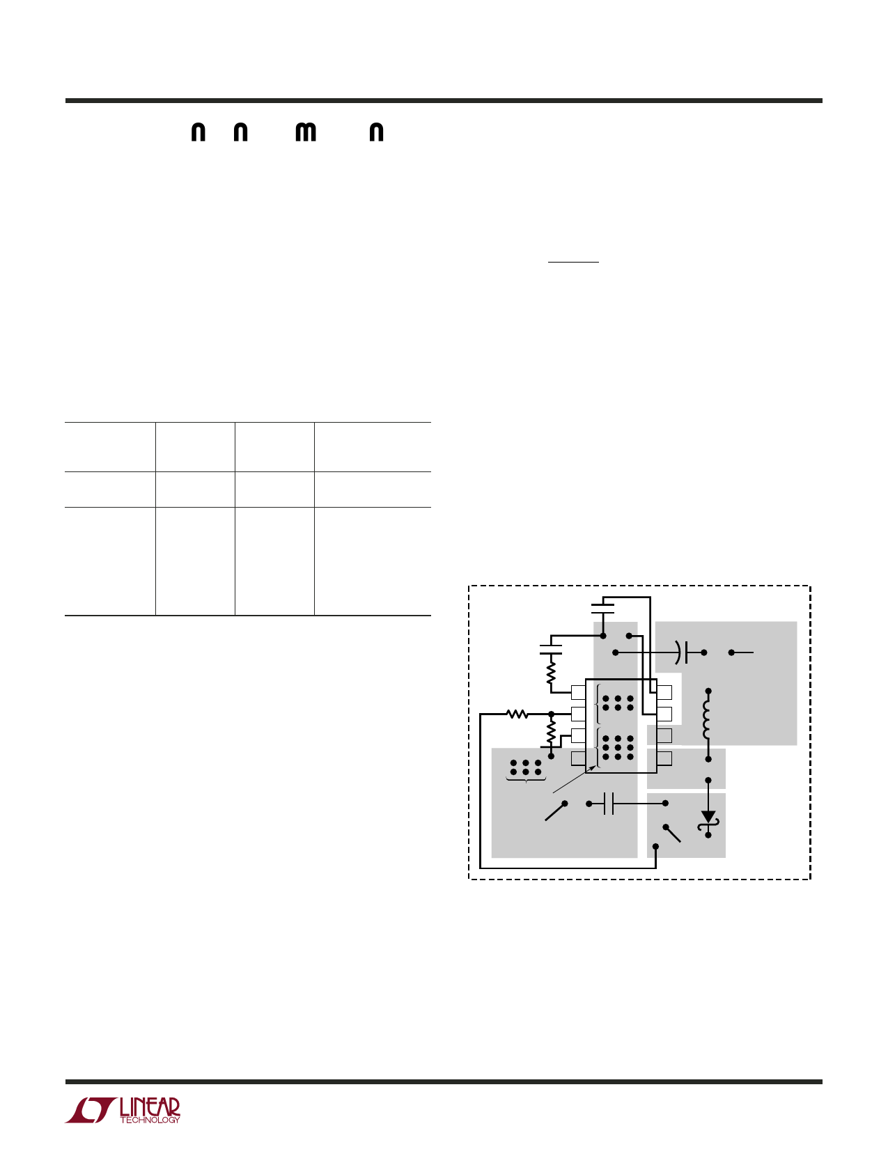
Board Layout
The high speed operation of the LT3489 demands care-
ful attention to board layout. For high-current switching
regulators like the LT3489, the board layout must have
good thermal performance. Vias located underneath the
part should be connected to an internal ground plane to
improve heat transfer from the LT3489 to the PCB board.
You will not get advertised performance with careless lay-
out. Thermal and noise consideration must be taken into
account. Figure 2 shows the recommended component
placement for a boost converter.
GROUND PLANE
CSS
C1
CC
+
VIN
RC
R1
R2
SHUTDOWN
1
2
LT3489
3
4
8
7 L1
6
5
MULTIPLE
VIAs
GND
C2
VOUT
3489 F02
Figure 2. Recommended Component Placement for Boost Converter.
Note Direct High Current Paths Using Wide PC Traces. Minimize
Trace Area at Pin 1 (VC) and Pin 2 (FB). Use Multiple Vias to Tie
Pin 4 Copper to Ground Plane. Use Vias at One Location Only to
Avoid Introducing Switching Currents Into the Ground Plane
3489f
7
Share Link: 