LT3489 Ver la hoja de datos (PDF) - Linear Technology
Número de pieza
componentes Descripción
Fabricante
LT3489 Datasheet PDF : 12 Pages
| |||
LT3489
ABSOLUTE AXI U RATI GS
(Note 1)
VIN Voltage................................................................16V
SW Voltage ................................................ –0.4V to 40V
FB, VC, COMP, SS Voltages .........................................6V
SHDN Voltage ...........................................................16V
Current Into FB Pin ................................................±1mA
Maximum Junction Temperature .......................... 125°C
Operating Temperature Range (Note 2) ... –40°C to 85°C
Storage Temperature Range................... –65°C to 150°C
Lead Temperature (Soldering, 10 sec) .................. 300°C
UW U
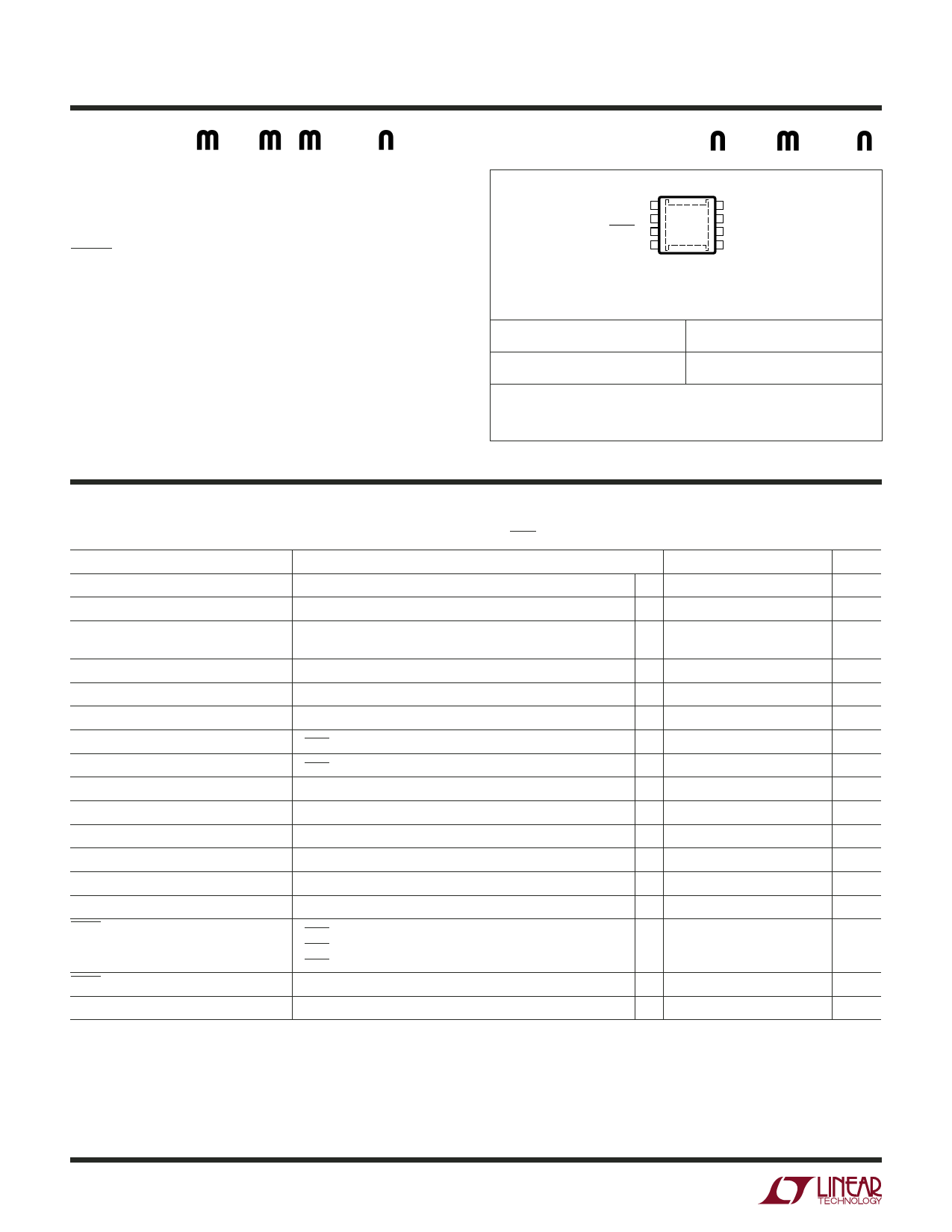
PACKAGE/ORDER I FOR ATIO
TOP VIEW
VC 1
FB 2
SHDN 3
GND 4
8 SS
7 COMP
6 VIN
5 SW
MS8E PACKAGE
8-LEAD PLASTIC MSOP
TJMAX = 125°C, θJA = 40°C/W, θJC = 10°C/W
EXPOSED PAD (PIN 9) IS GND (MUST BE SOLDERED TO PCB)
ORDER PART NUMBER MS8E PART MARKING
LT3489EMS8E
LTBYF
Order Options Tape and Reel: Add #TR
Lead Free: Add #PBF Lead Free Tape and Reel: Add #TRPBF
Lead Free Part Marking: http://www.linear.com/leadfree/
Consult LTC Marketing for parts specified with wider operating temperature ranges.
ELECTRICAL CHARACTERISTICS The ● denotes the specifications which apply over the full operating
temperature range, otherwise specifications are at TA = 25°C. VIN = 3V, VSHDN = VIN unless otherwise noted. (Note 2)
PARAMETER
CONDITIONS
MIN TYP MAX UNITS
Minimum Operating Voltage
2.4
2.6
V
Maximum Operating Voltage
16
V
Feedback Voltage
1.22 1.235 1.26
V
● 1.21
1.26
V
FB Pin Bias Current
Error Amp Transconductance
VFB = 1.25V (Note 3)
ΔI = 10μA
●
100
250
nA
100
μmhos
Error Amp Voltage Gain
80
V/V
Quiescent Current
Quiescent Current in Shutdown
Reference Line Regulation
Switching Frequency
VSHDN = 2.5V, Not Switching
VSHDN = 0V, VIN = 3V
2.6V ≤ VIN ≤ 16V
2
4
mA
0
1
μA
0.01 0.05
%
● 1.8
2
2.2
MHz
Maximum Switch Duty Cycle
● 85
90
%
Switch Current Limit
(Note 4)
● 2.5
3.5
5
A
Switch VCESAT
Switch Leakage Current
SHDN Pin Current
SHDN Pin Threshold
ISW = 2A
VSW = 5V
VSHDN = 5V
VSHDN = 1.4V
VSHDN = 0V
0.23
V
0.01
1
μA
100
μA
20
μA
2
μA
0.3
1.5
2
V
Soft-Start Charging Current
VSS = 0.5V
5
10
20
μA
Note 1: Stresses beyond those listed under Absolute Maximum Ratings
may cause permanent damage to the device. Exposure to any Absolute
Maximum Rating condition for extended periods may affect device
reliability and lifetime.
Note 2: The LT3489E is guaranteed to meet performance specifications
from 0°C to 70°C. Specifications over the 40°C to 85°C operating
temperature range are assured by design, characterization and correlation
with statistical process controls.
Note 3: Current flows out of the FB pin.
Note 4: Current limit guaranteed by design and/or correlation to static test.
Current limit is independent of duty cycle and is guaranteed by design.
3489f
2
Share Link: 