LT3469 Ver la hoja de datos (PDF) - Linear Technology
Número de pieza
componentes Descripción
Fabricante
LT3469 Datasheet PDF : 8 Pages
| |||
LT3469
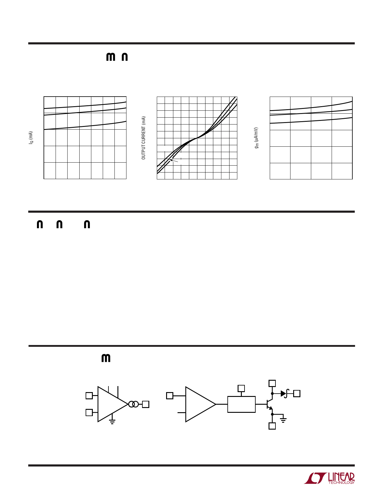
TYPICAL PERFOR A CE CHARACTERISTICS
(gm Amplifier)
VCC Quiescent Current
2.5
100°C
2.0
25°C
–50°C
1.5
1.0
0.5
0
15 18 21 24 27 30 33 36
VCC (V)
3469 G01
Output Current
vs Differential Input Voltage
30
25
20
15
10
5
0
–5
100°C
–10
–50°C
–15
25°C
–20
–25
–30
–50 –40 –30 –20 –10 0 10 20 30 40 50
DIFFERENTIAL INPUT VOLTAGE (mV)
3469 G02
gm vs VCC
250
200
150
–50°C
25°C
100°C
100
50
0
15
20
25
30
35
VCC (V)
3469 G14
PI FU CTIO S
OUT (Pin 1): Output of the gm Amplifier. There must be at
least 5nF of capacitive load at the output in a gain of 10
configuration. Capacitive loads up to 300nF can be con-
nected to this pin. Piezo actuators below 5nF can be driven
if capacitance is placed in parallel to bring the total
capacitance to 5nF.
FB (Pin 2): Feedback Pin. Reference voltage is 1.23V.
Connect feedback resistor divider here.
VIN (Pin 3): Input Supply Pin. Must be locally bypassed.
GND (Pin 4): Ground Pin. Connect directly to local ground
plane.
SW (Pin 5): Switch Pin. Connect inductor here. Minimize
trace area at this pin to reduce EMI.
VCC (Pin 6): Output of Switching Regulator and Supply
Rail for gm Amp. There must be 0.22µF or more of
capacitance here.
+IN (Pin 7): Noninverting Terminal of the gm Amplifier.
–IN (Pin 8): Inverting Terminal of the gm Amplifier.
BLOCK DIAGRA
VIN VCC
+IN
7+
–IN
gm
8–
FB
OUT
2
–
1
A1
1.23V
+
VIN
3
SWITCH
CONTROLLER
Figure 1. LT3469 Block Diagram
SW
5
VCC
6
Q1
4
3469 F01
GND
3469f
4
Share Link: 