LT3469 Ver la hoja de datos (PDF) - Linear Technology
Número de pieza
componentes Descripción
Fabricante
LT3469 Datasheet PDF : 8 Pages
| |||
LT3469
ABSOLUTE AXI U RATI GS
(Note 1)
VIN Voltage ............................................................. 16V
SW Voltage ............................................................. 40V
VCC Voltage............................................................. 38V
+IN, –IN Voltage ..................................................... 10V
FB Voltage ................................................................ 3V
Current Into SW Pin ................................................. 1A
Operating Temperature Range (Note 2) .. – 40°C to 85°C
Storage Temperature Range ................ – 65°C to 150°C
Lead Temperature (Soldering, 10 sec)................. 300°C
UW U
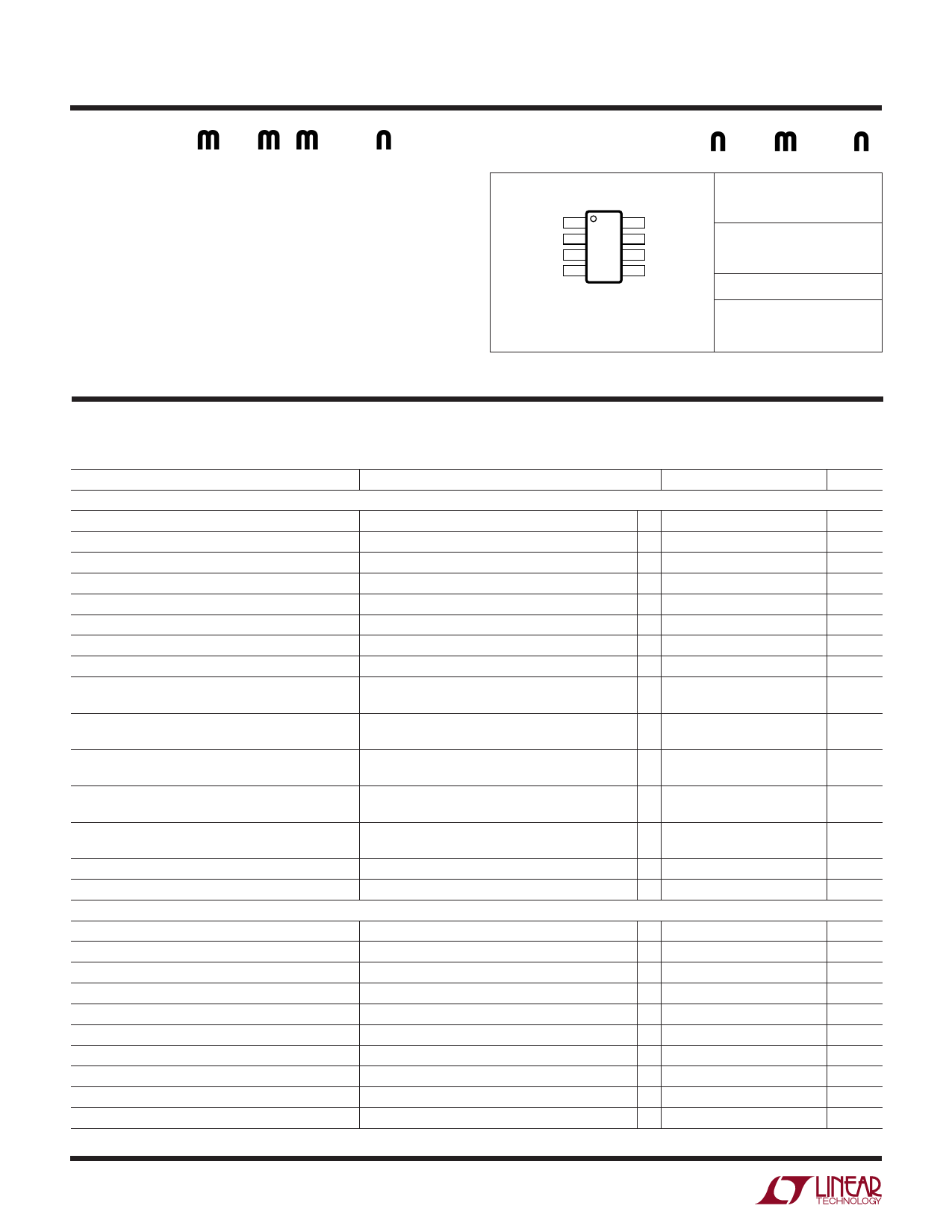
PACKAGE/ORDER I FOR ATIO
TOP VIEW
OUT 1
FB 2
VIN 3
GND 4
8 –IN
7 +IN
6 VCC
5 SW
TS8 PACKAGE
8-LEAD PLASTIC TSOT-23
TJMAX = 125°C, θJA = 250°C/W
ORDER PART
NUMBER
LT3469ETS8
TS8 PART MARKING
LTACA
Consult LTC Marketing for parts specified with wider operating temperature ranges.
ELECTRICAL CHARACTERISTICS The q denotes the specifications which apply over the full operating
temperature range, otherwise specifications are at TA = 25°C. (Note 2) VIN = 5V, VCC = 35V, unless otherwise noted.
PARAMETER
CONDITIONS
MIN TYP MAX
gm Amplifier
Input Offset Voltage
Input Offset Current
VOUT = VCC/2
q
3
10
q
10
100
Input Bias Current
q
150 500
Input Resistance—Differential Mode
1
Input Resistance—Common Mode
200
Common Mode Rejection Ratio
Power Supply Rejection Ratio—VIN
Power Supply Rejection Ratio—VCC
Gain
Transconductance
VCM = 0V to 10V
VIN = 2.5V to 16V
VCC = 15V to 35V
No Load, VOUT = 2V to 33V
RL = 200k, VOUT = 2V to 33V
IOUT = ±100µA
70
100
80
120
65
85
15
30
10
20
160 220 260
q 140
300
Maximum Output Current
VOUT = VCC/2
±30 ±40 ±55
q ±23
±58
Maximum Output Voltage, Sourcing
Minimum Output Voltage, Sinking
Output Resistance
Supply Current—VCC
Switching Regulator
VCC = 35V, IOUT = 10mA
VCC = 35V, IOUT = 0mA
IOUT = –10mA
IOUT = 0mA
VCC = 35V, VOUT = 2V to 33V
VCC = 35V
34.0 34.5
34.5 34.9
200 1000
10
500
100
1.5
2
2.5
Minimum Operating Voltage
2.5
Maximum Operating Voltage
16
Feedback Voltage
q 1.19 1.23 1.265
FB Pin Bias Current
q
45
200
FB Line Regulation
Supply Current—VIN
Switching Frequency
2.5V < VIN < 16V
0.03
1.9
2.6
q 0.8
1.3
1.7
Maximum Duty Cycle
q 88
91
Switch Current Limit (Note 3)
q 165
220
Switch VCESAT
ISW = 100mA
350 500
UNITS
mV
nA
nA
MΩ
MΩ
dB
dB
dB
V/mV
V/mV
µA/mV
µA/mV
mA
mA
V
V
mV
mV
kΩ
mA
V
V
V
nA
%/V
mA
MHz
%
mA
mV
3469f
2
Share Link: 