LT3468 Ver la hoja de datos (PDF) - Linear Technology
Número de pieza
componentes Descripción
Fabricante
LT3468 Datasheet PDF : 12 Pages
| |||
U
OPERATIO
The LT3468/LT3468-1/LT3468-2 are designed to charge
photoflash capacitors quickly and efficiently. The opera-
tion of the part can be best understood by referring to
Figure 1. When the CHARGE pin is first driven high, a one
shot sets both SR latches in the correct state. The power
NPN device, Q1, turns on and current begins ramping up
in the primary of transformer T1. Comparator A1 monitors
the switch current and when the peak current reaches 1.4A
(LT3468), 1A(LT3468-2) or 0.7A (LT3468-1), Q1 is turned
off. Since T1 is utilized as a flyback transformer, the
flyback pulse on the SW pin will cause the output of A3 to
be high. The voltage on the SW pin needs to be at least
36mV higher than VIN for this to happen.
During this phase, current is delivered to the photoflash
capacitor via the secondary and diode D1. As the second-
ary current decreases to zero, the SW pin voltage will begin
to collapse. When the SW pin voltage drops to 36mV
above VIN or lower, the output of A3 (DCM Comparator)
will go low. This fires a one shot which turns Q1 back on.
This cycle will continue to deliver power to the output.
Output voltage detection is accomplished via R2, R1, Q2,
and comparator A2 (VOUT Comparator). Resistors R1 and
R2 are sized so that when the SW voltage is 31.5V above
VIN, the output of A2 goes high which resets the master
latch. This disables Q1 and halts power delivery. NPN
transistor Q3 is turned on pulling the DONE pin low,
LT3468/LT3468-1/LT3468-2
indicating that the part has finished charging. Power
delivery can only be restarted by toggling the CHARGE pin.
The CHARGE pin gives full control of the part to the user.
The charging can be halted at any time by bringing the
CHARGE pin low. Only when the final output voltage is
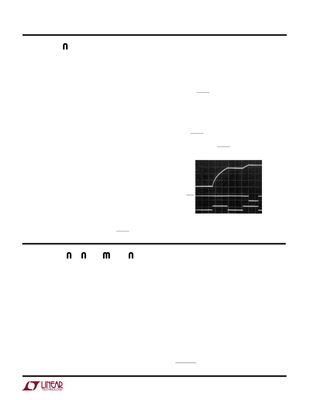
reached will the DONE pin go low. Figure 2 shows these
various modes in action. When CHARGE is first brought
high, charging commences. When CHARGE is brought
low during charging, the part goes into shutdown and
VOUT no longer rises. When CHARGE is brought high
again, charging resumes. When the target VOUT voltage is
reached, the DONE pin goes low and charging stops.
Finally the CHARGE pin is brought low again so the part
enters shutdown and the DONE pin goes high.
VOUT
100V/DIV
LT3468-2
VIN = 3.6V
COUT = 50µF
VDONE
5V/DIV
VCHARGE
5V/DIV
1s/DIV
3468 F02
Figure 2. Halting the Charging Cycle with the CHARGE Pin.
APPLICATIO S I FOR ATIO
Choosing The Right Device (LT3468/LT3468-1/
LT3468-2)
The only difference between the three versions of the
LT3468 is the peak current level. For the fastest possible
charge time, use the LT3468. The LT3468-1 has the lowest
peak current capability, and is designed for applications
that need a more limited drain on the batteries. Due to the
lower peak current, the LT3468-1 can use a physically
smaller transformer. The LT3468-2 has a current limit in
between that of the LT3468 and the LT3468-1.
Transformer Design
The flyback transformer is a key element for any LT3468/
LT3468-1/LT3468-2 design. It must be designed carefully
and checked that it does not cause excessive current or
voltage on any pin of the part. The main parameters that
need to be designed are shown in Table 1.
The first transformer parameter that needs to be set is the
turns ratio N. The LT3468/LT3468-1/LT3468-2 accom-
plish output voltage detection by monitoring the flyback
waveform on the SW pin. When the SW voltage reaches
31.5V higher than the VIN voltage, the part will halt power
delivery. Thus, the choice of N sets the target output
voltage as it changes the amplitude of the reflected voltage
from the output to the SW pin. Choose N according to the
following equation:
N = VOUT + 2
31. 5
346812f
7
Share Link: 