LT3467AIDDB-TRPBF(RevD) Ver la hoja de datos (PDF) - Linear Technology
Número de pieza
componentes Descripción
Fabricante
LT3467AIDDB-TRPBF
(Rev.:RevD)
(Rev.:RevD)
Linear Technology

LT3467AIDDB-TRPBF Datasheet PDF : 16 Pages
| |||
LT3467/LT3467A
APPLICATIONS INFORMATION
LOAD CURRENT
100mA/DIV
AC COUPLED
VOUT
200mV/DIV
AC COUPLED
IL1
5A/DIV
AC COUPLED
20μs/DIV
3467 F03
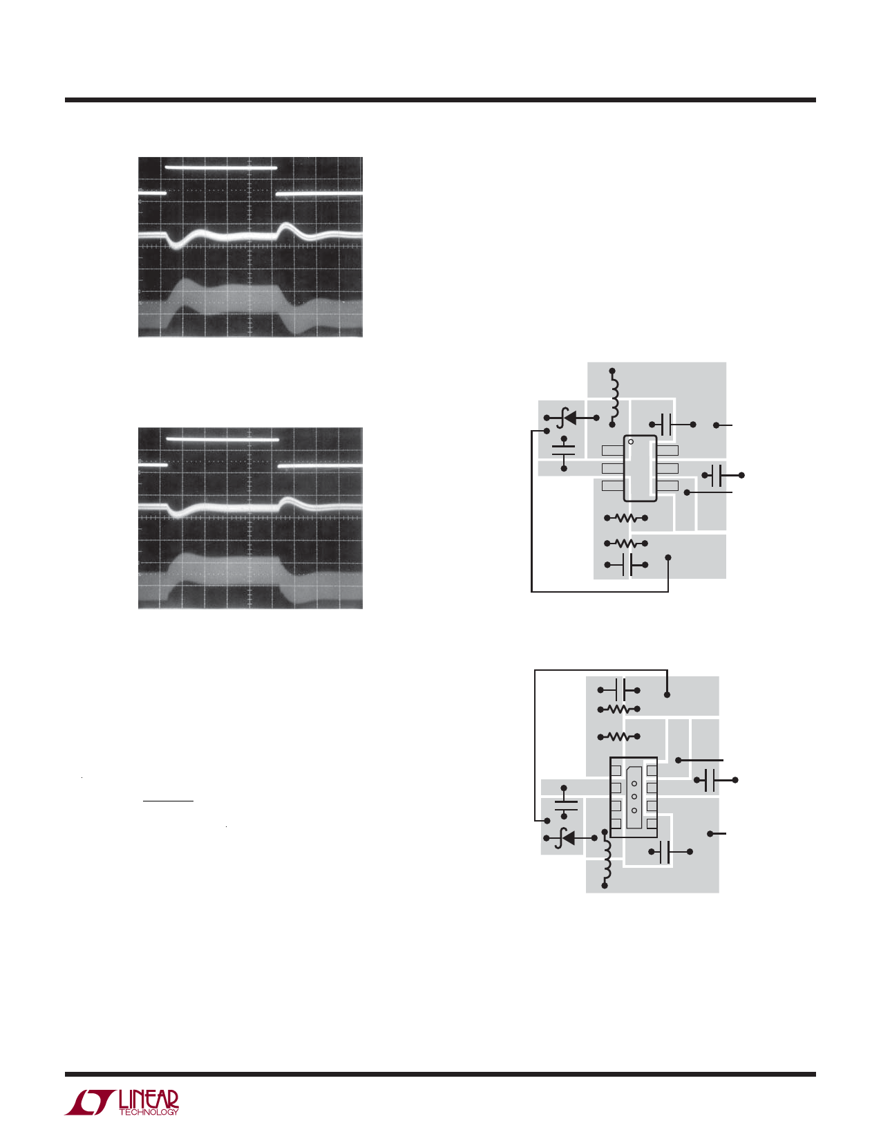
Figure 3. Transient Response of Figure 8’s Step-Up
Converter without Phase Lead Capacitor
LOAD CURRENT
100mA/DIV
AC COUPLED
VOUT
200mV/DIV
AC COUPLED
IL1
5A/DIV
AC COUPLED
20μs/DIV
3467 F04
Figure 4. Transient Response of Figure 8’s Step-Up
Converter with a 22pF Phase Lead Capacitor
Setting Output Voltage
To set the output voltage, select the values of R1 and R2
(see Figure 2) according to the following equation.
R1=
R2⎛⎝⎜
VOUT
1.255V
–
1⎞⎠⎟
A good value for R2 is 13.3k which sets the current in the
resistor divider chain to 1.255V/13.3k = 94μA.
Layout Hints
The high speed operation of the LT3467/LT3467A demands
careful attention to board layout. You will not get adver-
tised performance with careless layout. Figure 5a shows
the recommended component placement for the ThinSOT
package. Figure 5b shows the recommended component
placement for the DFN package. Note the vias under the
Exposed Pad. These should connect to a local ground
plane for better thermal performance.
L1
D1
VOUT
C2
1
2
GND
3
FB
C1
VIN
6
CSS
5 SS
4
SHDN
R2
R1
C3
VOUT 3467 F05a
Figure 5a. Suggested Layout—ThinSOT
GND
C2
VOUT
FB 1
2
3
4
D1
L1
VOUT
C3
R1
R2
8
7
CSS
6
5
C1
SHDN
VIN
3467 F05b
Figure 5b. Suggested Layout—DFN
3467afd
9
Share Link: