LT3466EDD-1 Ver la hoja de datos (PDF) - Linear Technology
NГәmero de pieza
componentes DescripciГіn
Fabricante
LT3466EDD-1 Datasheet PDF : 20 Pages
| |||
LT3466-1
ABSOLUTE AXI U RATI GS
(Note 1)
Input Voltage (VIN) ................................................... 24V
SW1, SW2 Voltages ................................................ 44V
VOUT1, VOUT2 Voltages ............................................. 44V
CTRL1, CTRL2 Voltages ........................................... 24V
FB1, FB2 Voltages ...................................................... 2V
Operating Temperature Range (Note 2) ... вҖ“40В°C to 85В°C
Storage Temperature Range .................. вҖ“65В°C to 125В°C
Junction Temperature .......................................... 125В°C
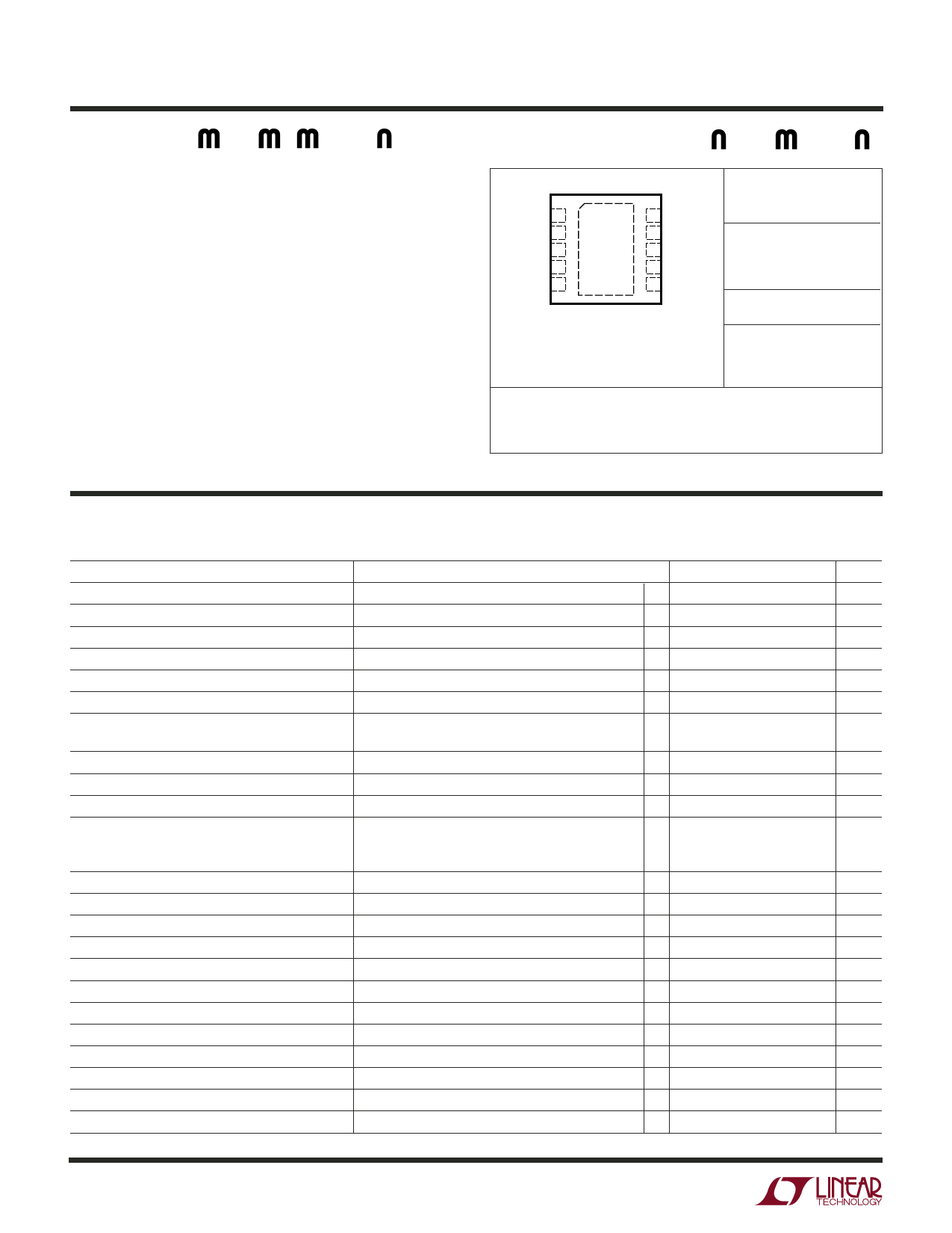
UW U
PACKAGE/ORDER I FOR ATIO
TOP VIEW
VOUT1 1
SW1 2
VIN 3
SW2 4
VOUT2 5
10 FB1
9 CTRL1
11
8 RT
7 CTRL2
6 FB2
DD PACKAGE
10-LEAD (3mm Г— 3mm) PLASTIC DFN
TJMAX = 125В°C, ОёJA = 43В°C/W, ОёJC = 3В°C/W
EXPOSED PAD (PIN 11) IS GND
MUST BE SOLDERED TO PCB
ORDER PART
NUMBER
LT3466EDD-1
DD PART MARKING
LBRX
Order Options Tape and Reel: Add #TR
Lead Free: Add #PBF Lead Free Tape and Reel: Add #TRPBF
Lead Free Part Marking: http://www.linear.com/leadfree/
Consult LTC Marketing for parts specified with wider operating temperature ranges.
ELECTRICAL CHARACTERISTICS The в—Ҹ denotes specifications that apply over the full operating temperature
range, otherwise specifications are at TA = 25В°C. VIN = 3V, VCTRL1 = 3V, VCTRL2 = 3V, unless otherwise specified.
PARAMETER
CONDITIONS
MIN TYP MAX UNITS
Minimum Operating Voltage
2.7
V
Maximum Operating Voltage
22
V
FB1 Voltage
в—Ҹ 192
200
208
mV
FB2 Voltage
в—Ҹ 788
800
812
mV
FB1 Pin Bias Current
FB2 Pin Bias Current
Quiescent Current
VFB1 = 0.2V (Note 3)
VFB2 = 0.8V (Note 3)
VFB1 = VFB2 = 1V
CTRL1 = CTRL2 = 0V
10
50
nA
10
50
nA
5
7.5
mA
16
25
ВөA
Switching Frequency
Oscillator Frequency Range
RT = 48.7k
(Note 4)
0.75
1
1.25
MHz
200
2000
kHz
Nominal RT Pin Voltage
Maximum Duty Cycle
Converter 1 Current Limit
RT = 48.7k
RT = 48.7k
RT = 20.5k
RT = 267k
0.54
V
в—Ҹ 90
96
%
92
%
99
%
в—Ҹ 310
400
mA
Converter 2 Current Limit
в—Ҹ 310
400
mA
Converter 1 VCESAT
Converter 2 VCESAT
Switch 1 Leakage Current
Switch 2 Leakage Current
CTRL1 Voltage for Full LED Current
ISW1 = 300mA
ISW2 = 300mA
VSW1 = 10V
VSW2 = 10V
320
mV
320
mV
0.01
5
ВөA
0.01
5
ВөA
в—Ҹ 1.8
V
CTRL2 Voltage for Full Feedback Voltage
в—Ҹ1
V
CTRL1 or CTRL2 Voltage to Turn On the IC
150
mV
CTRL1 and CTRL2 Voltages to Shut Down Chip
70
mV
CTRL1 Pin Bias Current
CTRL2 Pin Bias Current
VCTRL1 = 1V
VCTRL2 = 1V (Note 3)
в—Ҹ6
9
12.5
ВөA
в—Ҹ
10
120
nA
34661f
2
Share Link: 