LT3465 Ver la hoja de datos (PDF) - Linear Technology
Número de pieza
componentes Descripción
Fabricante
LT3465 Datasheet PDF : 12 Pages
| |||
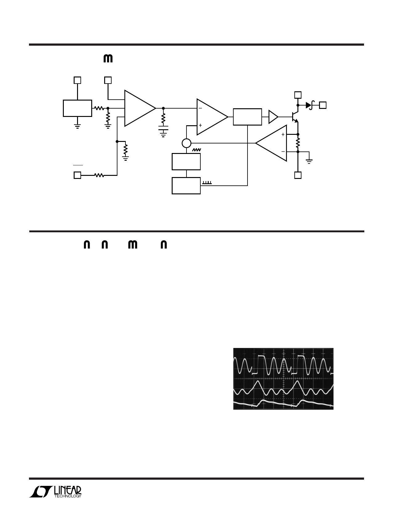
BLOCK DIAGRA
VIN
FB
5
3
VREF
1.25V
200mV
–
+ A1
+
10k
CTRL
40k
4
LT3465
– COMPARATOR
RC
A2
+
R
Q
S
CC
Σ
RAMP
GENERATOR
1.2MHz
OSCILLATOR
DRIVER
6 SW
Q1
VOUT
1
0.2Ω
2 GND
3465 F02
Figure 2. LT3465 Block Diagram
APPLICATIO S I FOR ATIO
Operation
The LT3465 uses a constant frequency, current mode
control scheme to provide excellent line and load regula-
tion. Operation can be best understood by referring to the
block diagram in Figure 2. At the start of each oscillator
cycle, the SR latch is set, which turns on the power switch
Q1. A voltage proportional to the switch current is added
to a stabilizing ramp and the resulting sum is fed into the
positive terminal of the PWM comparator A2. When this
voltage exceeds the level at the negative input of A2, the
SR latch is reset turning off the power switch. The level at
the negative input of A2 is set by the error amplifier A1,
and is simply an amplified version of the difference
between the feedback voltage and the reference voltage of
200mV. In this manner, the error amplifier sets the
correct peak current level to keep the output in regulation.
If the error amplifier’s output increases, more current is
delivered to the output; if it decreases, less current is
delivered. The CTRL pin voltage is used to adjust the
reference voltage.
Minimum Output Current
The LT3465 can drive a 3-LED string at 1.5mA LED
current without pulse skipping. As current is further
reduced, the device will begin skipping pulses. This will
result in some low frequency ripple, although the LED
current remains regulated on an average basis down to
zero. The photo in Figure 3 details circuit operation
driving three white LEDs at a 1.5mA load. Peak inductor
current is less than 40mA and the regulator operates in
VSW
5V/DIV
IL
20mA/DIV
VOUT
10mV/DIV
VIN = 4.2V
ILED = 1.5mA
3 LEDs
0.2µs/DIV
3465 F03
Figure 3. Switching Waveforms
sn3465 3465is
5
Share Link: 