LT3462 Ver la hoja de datos (PDF) - Linear Technology
Número de pieza
componentes Descripción
Fabricante
LT3462 Datasheet PDF : 8 Pages
| |||
LT3462/LT3462A
APPLICATIO S I FOR ATIO
Inrush Current
The LT3462 has a built-in Schottky diode. When supply
voltage is applied to the VIN pin, the voltage difference
between VIN and VD generates inrush current flowing from
input through the inductor and the Schottky diode to
charge the flying capacitor to VIN. The maximum
nonrepetitive surge current the Schottky diode in the
LT3462 can sustain is 1.5A. The selection of inductor and
capacitor value should ensure the peak of the inrush
current to be below 1.5A. The peak inrush current can be
calculated as follows:
IP
=
VIN – O.6
L –1
C
exp
–
2
π
L
C
–
1
where L is the inductance between supply and SW, and C
is the capacitance between SW and D.
Table 3 gives inrush peak currents for some component
selections.
Table 3. Inrush Peak Current
VIN (V)
5
L (µH)
22
5
33
12
47
C (µF)
1
1
1
IP (A)
0.70
0.60
1.40
Inductor Selection
Each of the two inductors used with LT3462 should have
a saturation current rating (where inductance is approxi-
mately 70% of zero current inductance ) of approximately
0.25A or greater. If the device is used in the charge pump
mode, where there is only one inductor, then its rating
should be 0.35A or greater. DCR of the inductors should
be less than 1Ω. For LT3462, a value of 22µH is suitable
if using a coupled inductor such as Sumida CLS62-220. If
using two separate inductors, increasing the value to
47µH will result in the same ripple current. For LT3462A,
a value of 10µH for the coupled inductor and 22µH for two
inductors will be acceptable for most applications.
Capacitor Selection
Ceramic capacitors are recommended. An X7R or X5R
dielectric should be used to avoid capacitance decreasing
severely with applied voltage and at temperature limits.
The “flying” capacitor between the SW and D pins should
be a ceramic type of value 1µF or more. When used in the
dual inductor or coupled inductor topologies the flying
capacitor should have a voltage rating that is more than the
difference between the input and output voltages. For the
charge pump inverter topology, the voltage rating should
be more than the output voltage. The output capacitor
should be a ceramic type. Acceptable output capacitance
varies from 1µF for high VOUT (–36V), to 10µF for low VOUT
(–5V). The input capacitor should be a 1µF ceramic type
and be placed as close as possible to the LT3462/LT3462A.
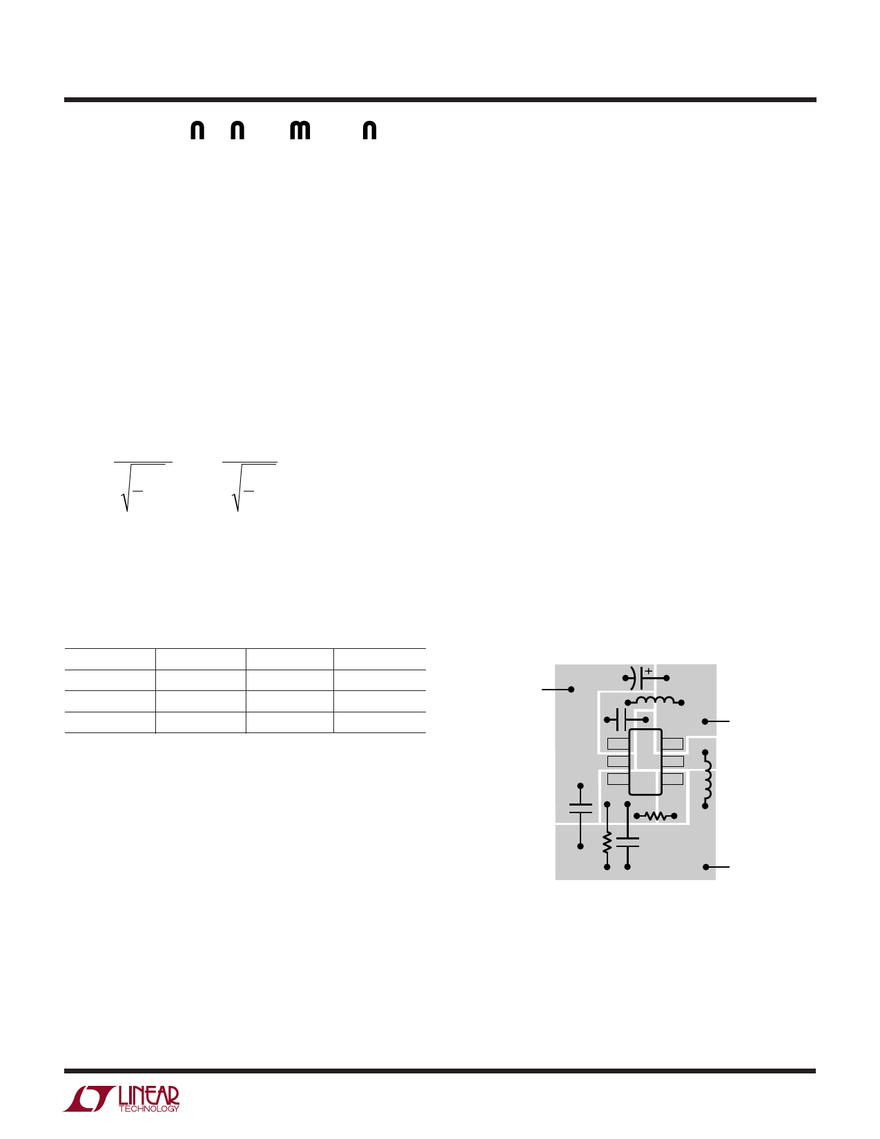
Layout Hints
The high speed operation of the LT3462 demands careful
attention to board layout. You will not get advertised
performance with careless layout. Figure 2 shows the
recommended component placement. A ceramic capaci-
tor of 1µF or more must be placed close to the IC for input
supply bypassing.
C1
GND
L1
C2
VIN
1
6
2
5
3
4 L2
C3
R2
R1
C4
3462 F03
VOUT
Figure 2. Suggested Layout
3462af
5
Share Link: 