LT1946 Ver la hoja de datos (PDF) - Linear Technology
Número de pieza
componentes Descripción
Fabricante
LT1946 Datasheet PDF : 12 Pages
| |||
LT1946
APPLICATIO S I FOR ATIO
Compensation—Theory
Like all other current mode switching regulators, the
LT1946 needs to be compensated for stable and efficient
operation. Two feedback loops are used in the LT1946: a
fast current loop which does not require compensation,
and a slower voltage loop which does. Standard Bode plot
analysis can be used to understand and adjust the voltage
feedback loop.
As with any feedback loop, identifying the gain and phase
contribution of the various elements in the loop is critical.
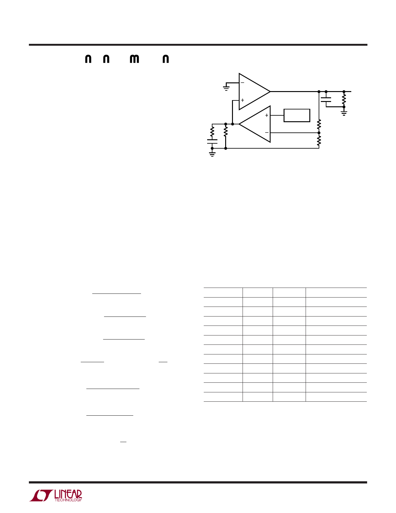
Figure 4 shows the key equivalent elements of a boost
converter. Because of the fast current control loop, the
power stage of the IC, inductor and diode have been
replaced by the equivalent transconductance amplifier
gmp. gmp acts as a current source where the output current
is proportional to the VC voltage. Note that the maximum
output current of gmp is finite due to the current limit in the
IC.
From Figure 4, the DC gain, poles and zeroes can be
calculated as follows:
Output Pole: P1=
2
2 • π • RL • COUT
Error Amp Pole: P2 =
1
2 • π • RO • CC
Error Amp Zero: Z1=
1
2 • π • RC • CC
DC
GAIN:
A
=
1.25VIN
2
VOUT
•
gma
• RO
•
gmp
•
RL
2
ESR Zero: Z2 =
1
2 • π • ESR • COUT
2
RHP Zero: Z3 = VIN • RL
2 • π • VOUT2 • L
High Frequency Pole: P3 > fS
3
–
gmp
+
VOUT
COUT RL
VC
gma
RC RO
1.250V
REFERENCE
R1
CC
R2
1946 F04
CC: COMPENSATION CAPACITOR
COUT: OUTPUT CAPACITOR
gma: TRANSCONDUCTANCE AMPLIFIER INSIDE IC
gmp: POWER STAGE TRANSCONDUCTANCE AMPLIFIER
RC: COMPENSATION RESISTOR
RL: OUTPUT RESISTANCE DEFINED AS VOUT DIVIDED BY ILOAD(MAX)
RO: OUTPUT RESISTANCE OF gma
R1, R2: FEEDBACK RESISTOR DIVIDER NETWORK
Figure 4. Boost Converter Equivalent Model
The Current Mode zero is a right half plane zero which can
be an issue in feedback control design, but is manageable
with proper external component selection.
Using the circuit of Figure 1 as an example, the following
table shows the parameters used to generate the Bode plot
shown in Figure 5.
Table 3. Bode Plot Parameters
Parameter
Value
Units
RL
18.6
Ω
COUT
20
µF
RO
10
MΩ
CC
470
pF
RC
49.9
kΩ
VOUT
8
V
VIN
3.3
V
gma
40
µmho
gmp
5
mho
L
5.4
µH
fS
1.2
MHz
Comment
Application Specific
Application Specific
Not Adjustable
Adjustable
Adjustable
Application Specific
Application Specific
Not Adjustable
Not Adjustable
Application Specific
Not Adjustable
From Figure 5, the phase is 120° when the gain reaches
0dB giving a phase margin of 60°. This is more than
adequate. The crossover frequency is 25kHz, which is
about three times lower than the frequency of the right half
plane zero Z2. It is important that the crossover frequency
be at least three times lower than the frequency of the RHP
zero to achieve adequate phase margin.
1946fb
7
Share Link: 