LT1946 Ver la hoja de datos (PDF) - Linear Technology
Número de pieza
componentes Descripción
Fabricante
LT1946 Datasheet PDF : 12 Pages
| |||
LT1946
PI FU CTIO S
VC (Pin 1): Error Amplifier Output Pin. Tie external com-
pensation network to this pin, or use the internal compen-
sation network by shorting the VC pin to the COMP pin.
FB (Pin 2): Feedback Pin. Reference voltage is 1.250V.
Connect resistive divider tap here. Minimize trace area at
FB. Set VOUT according to VOUT = 1.250(1 + R1/R2).
SHDN (Pin 3): Shutdown Pin. Tie to 2.4V or more to enable
device. Ground to shut down. Do not float this pin.
GND (Pin 4): Ground. Tie directly to local ground plane.
SW (Pin 5): Switch Pin. This is the collector of the internal
NPN power switch. Minimize the metal trace area con-
nected to this pin to minimize EMI.
VIN (Pin 6): Input Supply Pin. Must be locally bypassed.
COMP (Pin 7): Internal Compensation Pin. Provides an
internal compensation network. Tie directly to the VC pin
for internal compensation. Tie to GND if not used.
SS (Pin 8): Soft-Start Pin. Place a soft-start capacitor
here. Upon start-up, 4µA of current charges the capacitor
to 1.5V. Use a larger capacitor for slower start-up. Leave
floating if not in use.
Exposed Pad (MS8E, Pin 9): Ground. Must be soldered to
PCB.
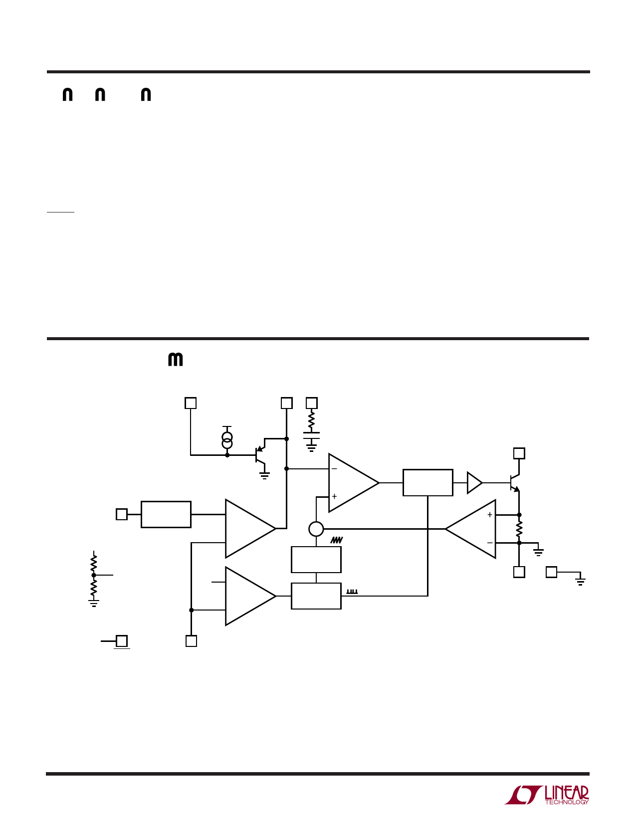
BLOCK DIAGRA
SS
8
4µA
VIN
6
1.250V
REFERENCE
VOUT
R1 (EXTERNAL)
FB
R2 (EXTERNAL)
0.5V
+
A1
–
+
A3
–
SHUTDOWN
3
2
SHDN
FB
VC COMP
1
7
120k
90pF
–
COMPARATOR
A2
+
R
Q
S
Σ
RAMP
GENERATOR
÷3 1.2MHz
OSCILLATOR
SW
5
DRIVER
Q1
0.01Ω
4
9
GND
GND
(MSE8 ONLY)
1946 BD
Figure 2. Block Diagram
1946fb
4
Share Link: 