LT1944 Ver la hoja de datos (PDF) - Linear Technology
Número de pieza
componentes Descripción
Fabricante
LT1944 Datasheet PDF : 8 Pages
| |||
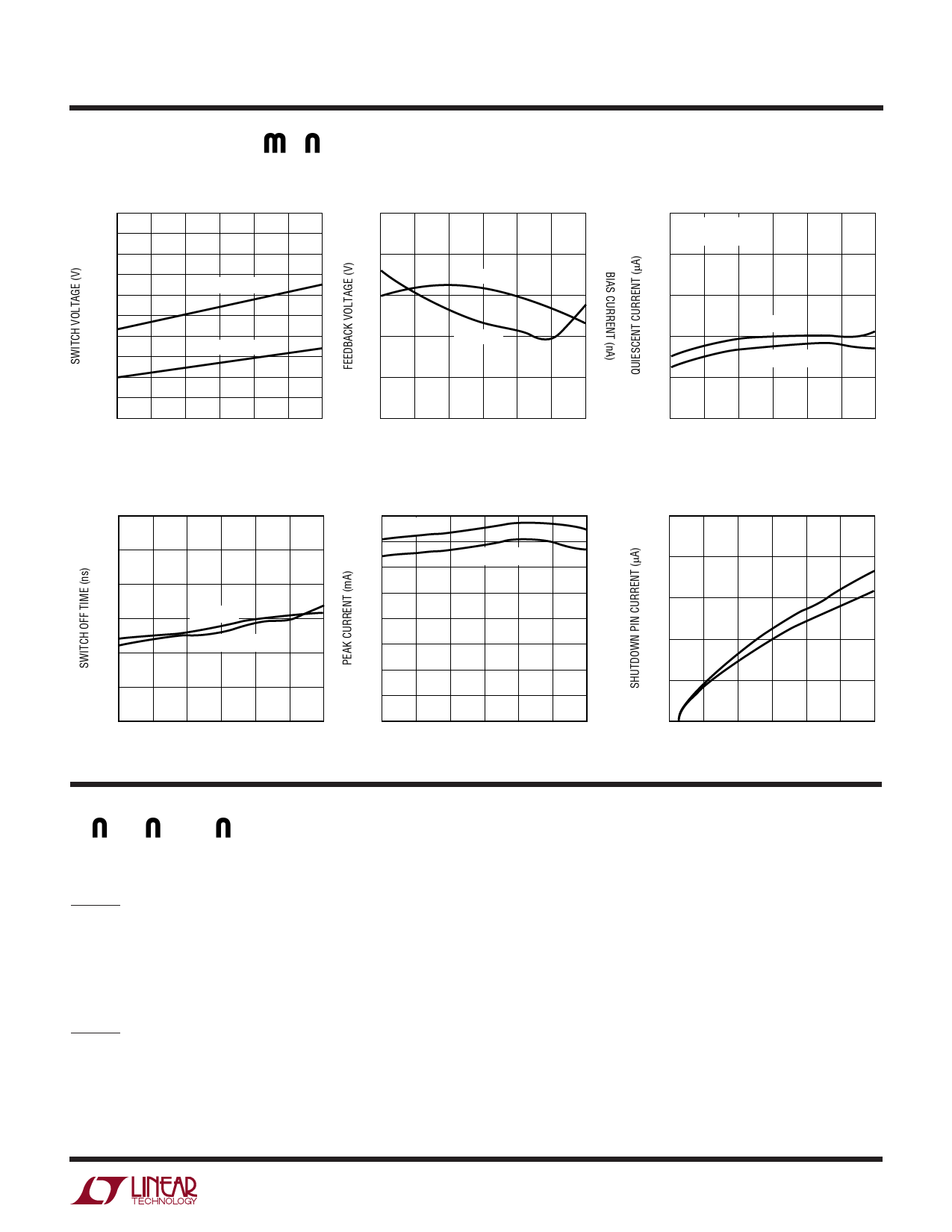
TYPICAL PERFOR A CE CHARACTERISTICS
Switch Saturation Voltage
(VCESAT)
0.60
0.55
0.50
0.45
ISWITCH = 500mA
0.40
0.35
0.30
ISWITCH = 300mA
0.25
0.20
0.15
0.10
–50 –25 0
25 50 75 100
TEMPERATURE (°C)
1944 G01
Feedback Pin Voltage and
Bias Current
1.25
50
1.24
40
VOLTAGE
1.23
30
1.22
CURRENT
20
1.21
10
1.20
–50
–25 0 25 50
TEMPERATURE (°C)
0
75 100
1944 G02
Switch Off Time
550
500
450
400
VIN = 1.2V
VIN = 12V
350
300
250
–50
–25 0 25 50
TEMPERATURE (°C)
75 100
1944 G04
Switch Current Limit
400
VIN = 12V
350
300
VIN = 1.2V
250
200
150
100
50
0
–50 –25 0
25 50 75 100
TEMPERATURE (°C)
1944 G05
LT1944
Quiescent Current
25
VFB = 1.23V
NOT SWITCHING
23
21
VIN = 12V
19
VIN = 1.2V
17
15
–50
–25 0 25 50
TEMPERATURE (°C)
75 100
1944 G03
Shutdown Pin Current
25
20
15
25°C
10
100°C
5
0
0
5
10
15
SHUTDOWN PIN VOLTAGE (V)
1944 G03
PI FU CTIO S
FB1 (Pin 1): Feedback Pin for Switcher 1. Set the output
voltage by selecting values for R1 and R2.
SHDN1 (Pin 2): Shutdown Pin for Switcher 1. Tie this pin
to 0.9V or higher to enable device. Tie below 0.25V to turn
it off.
GND (Pin 3): Ground. Tie this pin directly to the local
ground plane.
SHDN2 (Pin 4): Shutdown Pin for Switcher 2. Tie this pin
to 0.9V or higher to enable device. Tie below 0.25V to turn
it off.
FB2 (Pin 5): Feedback Pin for Switcher 2. Set the output
voltage by selecting values for R1B and R2B.
SW2 (Pin 6): Switch Pin for Switcher 2. This is the
collector of the internal NPN power switch. Minimize the
metal trace area connected to the pin to minimize EMI.
PGND (Pins 7, 9): Power Ground. Tie these pins directly
to the local ground plane. Both pins must be tied.
VIN (Pin 8): Input Supply Pin. Bypass this pin with a
capacitor as close to the device as possible.
SW1 (Pin 10): Switch Pin for Switcher 1. This is the
collector of the internal NPN power switch. Minimize the
metal trace area connected to the pin to minimize EMI.
3
Share Link: 