LT1940 Ver la hoja de datos (PDF) - Linear Technology
Número de pieza
componentes Descripción
Fabricante
LT1940 Datasheet PDF : 20 Pages
| |||
LT1940/LT1940L
APPLICATIO S I FOR ATIO
Table 2. Low-ESR Surface Mount Capacitors
Vendor
Type
Series
Taiyo Yuden
Ceramic X5R, X7R
AVX
Ceramic X5R, X7R
Tantalum
TPS
Kemet
Tantalum
Ta Organic
Al Organic
T491,T494,T495
T520
A700
Sanyo
Ta or Al Organic
POSCAP
Panasonic
Al Organic
SP CAP
TDK
Ceramic X5R, X7R
Catch Diode
Use a 1A Schottky diode for the catch diode (D1 in
Figure 2). The diode must have a reverse voltage rating
greater than the maximum input voltage. The ON Semi-
conductor MBRM120LT3 (20V) and MBRM130LT3 (30V)
are good choices; they have a tiny package with good
thermal properties. Many vendors have surface mount
versions of the 1N5817 (20V) and 1N5818 (30V) 1A
Schottky diodes such as the Microsemi UPS120 that are
suitable.
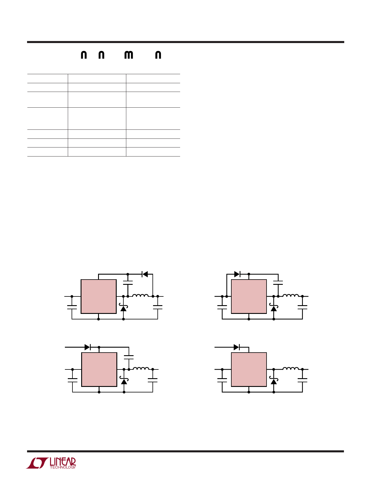
Boost Pin Considerations
The capacitor and diode tied to the BOOST pin generate a
voltage that is higher than the input voltage. In most cases
a 0.1µF capacitor and fast switching diode (such as the
CMDSH-3 or FMMD914) will work well. Figure 3 shows
three ways to arrange the boost circuit. The BOOST pin
must be more than 2.5V above the SW pin for full effi-
ciency. For outputs of 3.3V and higher the standard circuit
(Figure 3a) is best. For outputs between 2.8V and 3.3V,
use a small Schottky diode (such as the BAT-54). For lower
output voltages the boost diode can be tied to the input
(Figure␣ 3b). The circuit in Figure 3a is more efficient
because the BOOST pin current comes from a lower
voltage source. Finally, as shown in Figure 3c, the anode
of the boost diode can be tied to another source that is at
least 3V. For example, if you are generating 3.3V and 1.8V
and the 3.3V is on whenever the 1.8V is on, the 1.8V boost
diode can be connected to the 3.3V output. In any case,
you must also be sure that the maximum voltage at the
BOOST pin is less than the maximum specified in the
Absolute Maximum Ratings section.
D2
D2
BOOST
C3
LT1940
VIN
VIN
SW
GND
VOUT
BOOST
C3
LT1940
VIN
VIN
SW
GND
VOUT
VIN2 > 3V
VBOOST – VSW ≅ VOUT
MAX VBOOST ≅ VIN + VOUT
(3a)
D2
BOOST
C3
LT1940
VIN
VIN
SW
GND
VBOOST – VSW ≅ VIN2
MAX VBOOST ≅ VIN2 + VIN
MINIMUM VALUE FOR VIN2 = 3V
(3c)
VOUT
1940 F03
VIN2
>VIN + 3V
VIN
VBOOST – VSW ≅ VIN
MAX VBOOST ≅ 2VIN
(3b)
D2
BOOST
LT1940
VIN
SW
GND
MAX VBOOST – VSW ≅ VIN2
MAX VBOOST ≅ VIN2
MINIMUM VALUE FOR VIN2 = VIN + 3V
(3d)
VOUT
1940 F03
Figure 3. Generating the Boost Voltage
1940fa
11
Share Link: 