LT1619 Ver la hoja de datos (PDF) - Linear Technology
Número de pieza
componentes Descripción
Fabricante
LT1619 Datasheet PDF : 20 Pages
| |||
LT1619
U
OPERATIO
The LT1619 is a fixed frequency current mode switching
regulator PWM controller that can be used in boost, SEPIC
or flyback modes. The device operates from an input
supply range of 1.9V to 18V, and has a separate supply pin
(DRV) for the gate driver. The DRV pin can be bootstrapped
to VOUT for additional gate enhancement in low voltage
applications like 3.3V to 5V boost converters, or con-
nected to the input supply for higher voltage inputs.
To best understand operation of the LT1619, please refer
to Figure 2, the Block Diagram. The gate drive circuit turns
on the external MOSFET at the trailing edge of oscillator
output signal CLK. MOSFET current is sensed with an
external resistor (RSENSE of Figure 1). A leading edge
blanking circuit disables the current sense amplifier for
280ns immediately following switch turn-on, preventing
gate charging current from prematurely tripping the PWM
comparator. A slope compensating ramp, derived from
the oscillator, is added to the current sense output. The
driver turns off the MOSFET when this sum exceeds the
error amplifier output VC. The switch current is limited
with a separate comparator. The compensating ramp is a
progressive nonlinear function of the operating duty ratio
whereas the current limit does not vary with the duty ratio.
Error amplifier output VC determines the peak switch cur-
rent required to regulate the output voltage. VC can be
considered a measure of output current. At heavy loads,
VC is in its upper range. Average and peak inductor cur-
rents are high. In this range, the inductor tends to run in
continuous conduction mode (CCM), where current is al-
ways flowing in the inductor. As load current decreases,
average and peak inductor current decreases. When the
average inductor current falls below 1/2 of the peak-to-peak
inductor current ripple, the converter enters discontinu-
ous conduction mode (DCM), where current in the induc-
tor reaches zero sometime during the discharge phase.
Further reduction in output current moves VC towards its
lower operating range, decreasing inductor current. Hys-
teretic comparator A1 determines if VC is too low for the
LT1619 to operate efficiently. As VC falls below the trip
voltage VB, A1’s output goes high, turning off all blocks
except the error amplifier, A1 and A2. The LT1619 enters
the idle state and switching stops. The device draws just
140µA from the input in the idle state. Output load current
discharges the output capacitor, causing the output volt-
age to decrease. As VOUT decreases, VC increases. As VC
increases above VB, switching action begins, delivering
power to the output. The switch current sense threshold is
about 10mV in this VC region. If the output load remains
light, the output voltage will rise and VC will fall, causing
the converter to idle again. This is known as Burst Mode
operation. The burst frequency depends on input voltage,
output voltage, inductance and output capacitance. Out-
put voltage ripple during Burst Mode operation is usually
higher than when the converter is switching continuously.
Burst Mode operation increases light load efficiency be-
cause it delivers more energy per clock cycle than possible
with discontinuous mode operation and extremely low
peak switch current, allowing fewer switching cycles to
maintain a given output. IC supply current therefore be-
comes a small fraction of the total input current.
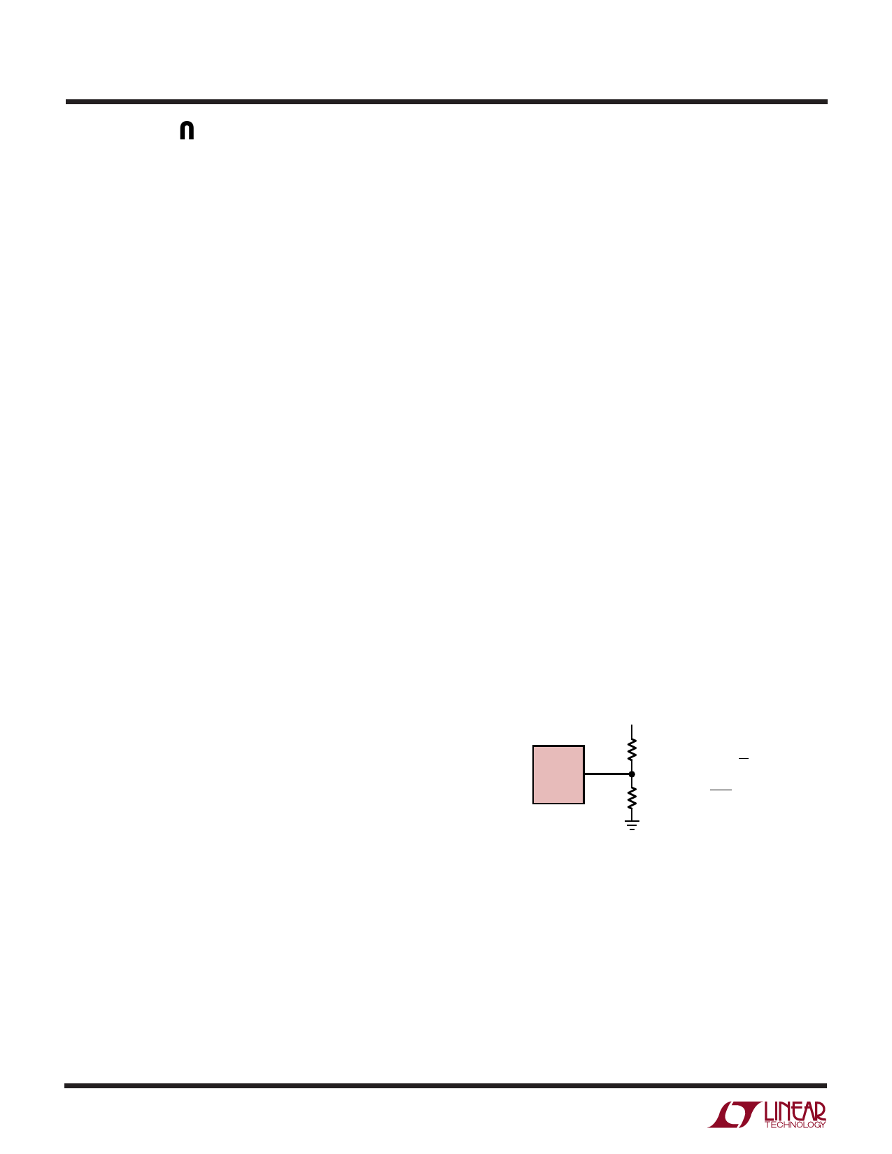
Setting Output Voltage
The output voltage of the LT1619 is set with resistive
divider R1 and R2 connected from the output to ground as
detailed in Figure 3. The divider tap is tied to the device FB
pin. Current through R2 should be significantly higher
than the FB pin bias current of 25nA. With R2 = 10k, the
input bias current of the error amplifier is 0.02% of the
current in R2.
LT1619
FB
VO
( ) R1
VO = 1.24V
1+
R1
R2
( ) R2
R1 = R2
VO
1.24
–1
1619 F03
Figure 3. Feedback Resistive Divider
Synchronization and Shutdown
The S/S pin (Pin 1) can be used to synchronize the
oscillator to an external source. The S/S pin is tied to the
input (VIN > 1.9V) for normal operation. The oscillator in
the LT1619 can be externally synchronized by driving the
S/S pin with a pulse train with an amplitude of at least 1V.
The maximum allowable rise time is a function of the
pulse amplitude, as shown in Table 1. Rise times equal to
6
Share Link: 