LT1619 Ver la hoja de datos (PDF) - Linear Technology
Número de pieza
componentes Descripción
Fabricante
LT1619 Datasheet PDF : 20 Pages
| |||
LT1619
ABSOLUTE AXI U RATI GS (Note 1)
Input Voltage (VIN) ................................... – 0.3V to 20V
Gate Drive Supply Voltage (DRV) ............. – 0.3V to 20V
Shutdown/Synch Voltage (S/S) ................ – 0.3V to 20V
Feedback Voltage (FB) .............................................. VIN
Compensation Voltage (VC) ...................................... 3V
Gate Drive Output Current (GATE) ........................ ±1.5A
Current Sense Voltage (SENSE) ................. – 0.5V to VIN
Operating Temperature Range (Note 2) .. – 40°C to 85°C
Junction Temperature (Note 3) ............................. 125°C
Storage Temperature Range ................. – 65°C to 150°C
Lead Temperature (Soldering, 10 sec).................. 300°C
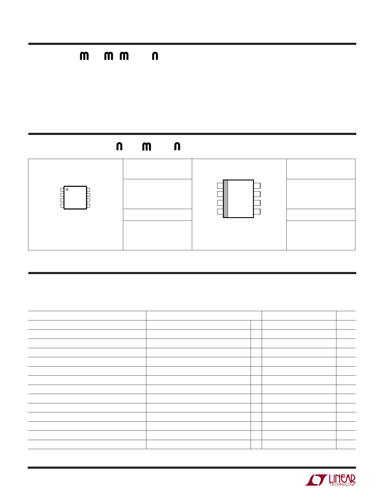
UW U
PACKAGE/ORDER I FOR ATIO
TOP VIEW
S/S 1
FB 2
VC 3
GND 4
8 VIN
7 DRV
6 GATE
5 SENSE
MS8 PACKAGE
8-LEAD PLASTIC MSOP
TJMAX = 125°C, θJA = 200°C/ W
ORDER PART
NUMBER
LT1619EMS8
MS8 PART MARKING
LTHC
Consult factory for Military grade parts.
TOP VIEW
S/S 1
FB 2
VC 3
GND 4
8 VIN
7 DRV
6 GATE
5 SENSE
S8 PACKAGE
8-LEAD PLASTIC SO
TJMAX = 125°C, θJA = 120°C/ W
ORDER PART
NUMBER
LT1619ES8
S8 PART MARKING
1619
ELECTRICAL CHARACTERISTICS
The q denotes specifications which apply over the full operating temperature range, otherwise specifications are at TA = 25°C.
VIN = VDRV = 2.5V, VS/S = VIN, COMP open, VSENSE = 0V unless otherwise noted.
PARAMETER
Reference Voltage
Reference Line Regulation
FB Input Bias Current
Error Amplifier Transconductance
Error Amplifier Output Source Current
Error Amplifier Output Sink Current
Error Amplifier Clamp Voltage
Undervoltage Lockout Threshold
Input Voltage Range
Switching Frequency
Synchronization Frequency Range
Maximum Duty Cycle
Current Limit Threshold
Burst Mode Operation Current Limit
CONDITIONS
Measured at the FB Pin
1.9V ≤ VIN ≤ 18V
VFB = VREF
VFB = 1V, VCOMP = 1V
VFB = 1.5V, VCOMP = 1V
VFB = 1V
1.9V ≤ VIN ≤ 18V
MIN TYP MAX
q 1.22 1.24 1.26
0.004 0.05
10
25
80
170
260
4
8.7
14
4
8.7
14
1.6
2.2
1.65
1.85
q
1.9
18
q
220
300
360
370
500
q
88
92
q
40
53
66
10
UNITS
V
%/V
nA
µΩ – 1
µA
µA
V
V
V
kHz
kHz
%
mV
mV
2
Share Link: 