LT1587-1.5 Ver la hoja de datos (PDF) - Linear Technology
Número de pieza
componentes Descripción
Fabricante
LT1587-1.5 Datasheet PDF : 8 Pages
| |||
LT1587-1.5
APPLICATIONS INFORMATION
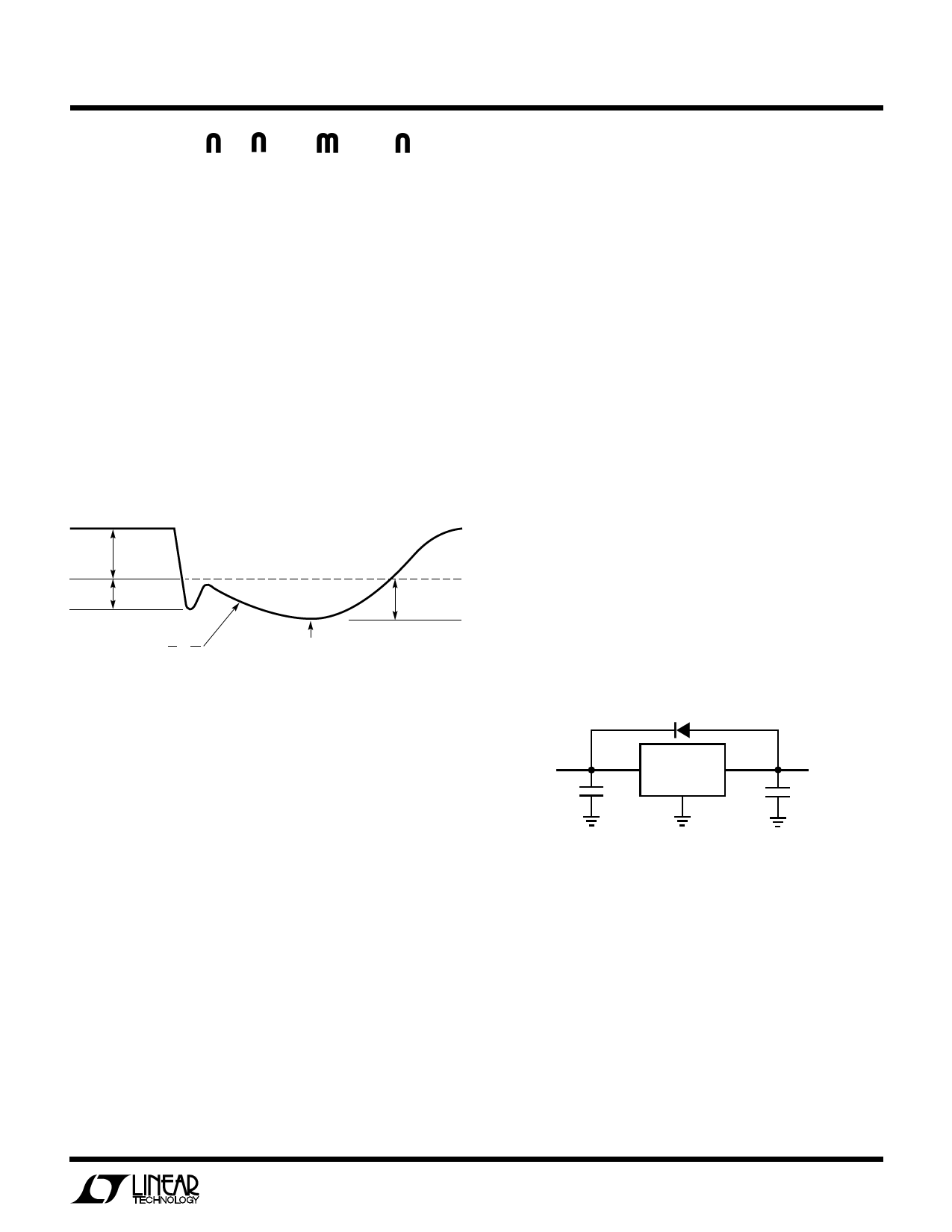
Large load current changes are exactly the situation pre-
sented by modern microprocessors and their peripheral
circuitry. The load current step contains higher order
frequency components that the output decoupling network
must handle until the regulator throttles to the load current
level. Capacitors are not ideal elements and contain para-
sitic resistance and inductance. These parasitic elements
dominate the change in output voltage at the beginning of
a transient load step change. The ESR of the output
capacitors produces an instantaneous step in output volt-
age [∆V = ∆I(ESR)]. The ESL of the output capacitors
produces a droop proportional to the rate of change of
output current [V = L(∆I/∆t)]. The output capacitance
produces a change in output voltage proportional to the
time until the regulator can respond [∆V = ∆t(∆I/C)]. These
transient effects are illustrated in Figure 1.
ESR
EFFECTS
ESL
EFFECTS
CAPACITANCE
EFFECTS
SLOPE,
V
t
=
∆I
C
POINT AT WHICH REGULATOR
TAKES CONTROL
Figure 1
LT1587 • F01
The use of capacitors with low ESR, low ESL and good high
frequency characteristics is critical in meeting the output
voltage tolerances of these high speed microprocessor
applications. These requirements dictate a combination of
high quality surface mount tantalum capacitors and ce-
ramic capacitors. The location of the decoupling network is
critical to transient response performance. Place the
decoupling network as close as possible to the micropro-
cessor control circuitry because a trace run from the
decoupling capacitors to the actual circuitry is inductive. In
addition, use large power and ground plane areas to
minimize distribution drops.
A possible stability problem that occurs in monolithic linear
regulators is current limit oscillations. The LT1587-1.5
essentially has a flat current limit over the range of input
supply voltage. The lower current limit rating and 7V
maximum supply voltage rating for this device permits this
characteristic. Current limit oscillations are typically non-
existent unless the input and output decoupling capacitors
for the regulators are mounted several inches from the
terminals.
Protection Diodes
In normal operation, the LT1587-1.5 does not require any
protection diodes. Older 3-terminal regulators require
protection diodes between the output pin and the input pin
to prevent die overstress.
A protection diode between the input and output pins is
usually not needed. An internal diode between the input
and output pins on the LT1587-1.5 can handle microsec-
ond surge currents of 50A to 100A. Even with large value
output capacitors it is difficult to obtain those values of
surge currents in normal operation. Only with large values
of output capacitance, such as 1000µF to 5000µF, and with
the input pin instantaneously shorted to ground can dam-
age occur. A crowbar circuit at the input of the LT1587-1.5
can generate those levels of current, and a diode from
output to input is then recommended. This is shown in
Figure 2. Usually, normal power supply cycling or system
“hot plugging and unplugging” will not generate current
large enough to do any damage.
D1
1N4002
(OPTIONAL)
LT1587-1.5
VIN
+ C1
IN
OUT
GND
10µF
+
VOUT
C2
10µF
LT1587 • F02
Figure 2
Ripple Rejection
The typical curve for ripple rejection reflects values for the
LT1587-1.5 as a function of frequency. In applications that
require improved ripple rejection, use the adjustable
LT1587. A bypass capacitor from the adjust pin to ground
reduces the output ripple by the ratio of VOUT/1.25V.
Load Regulation
It is not possible to provide true remote load sensing
because the LT1587-1.5 is a 3-terminal device. Load
5
Share Link: 