1506I Ver la hoja de datos (PDF) - Linear Technology
Número de pieza
componentes Descripción
Fabricante
1506I Datasheet PDF : 24 Pages
| |||
LT1506
APPLICATIONS INFORMATION
formulas show how to calculate each of these losses.
These formulas assume continuous mode operation, so
they should not be used for calculating efficiency at light
load currents.
Switch loss:
( ) ( ) ( )( )( ) 2
PSW
= RSW
IOUT
VIN
VOUT
+ 24ns IOUT
VIN
f
Boost current loss:
( ) PBOOST
=
VOUT2
IOUT
VIN
/ 50
Quiescent current loss:
( ) ( ) ( ) PQ
= VIN
0.001
+ VOUT
0.005
+
VOUT2
0.002
VIN
RSW = Switch resistance (≈ 0.07)
24ns = Equivalent switch current/voltage overlap time
f = Switch frequency
Example: with VIN = 10V, VOUT = 5V and IOUT = 3A:
( )( ) ( ) ( )( ) 2
0.07 3
PSW =
10
5
+
24
•
10−9
3
10
500
•
10
3
= 0.32 + 0.36 = 0.68W
(5)2(3/ 50)
PBOOST =
10
= 0.15W
( ) ( ) ( ) ( ) 2
5 0.002
PQ = 10 0.001 + 5 0.005 + 10 = 0.04W
Total power dissipation is 0.68 + 0.15 + 0.04 = 0.87W.
Thermal resistance for LT1506 package is influenced by
the presence of internal or backside planes. With a full
plane under the SO package, thermal resistance will be
about 80°C/W. No plane will increase resistance to about
120°C/W. To calculate die temperature, use the proper
thermal resistance number for the desired package and
add in worst-case ambient temperature:
TJ = TA + θJA (PTOT)
With the SO-8 package (θJA = 80°C/W), at an ambient
temperature of 50°C,
TJ = 50 + 80 (0.87) = 120°C
Die temperature is highest at low input voltage, so use
lowest continuous input operating voltage for thermal
calculations.
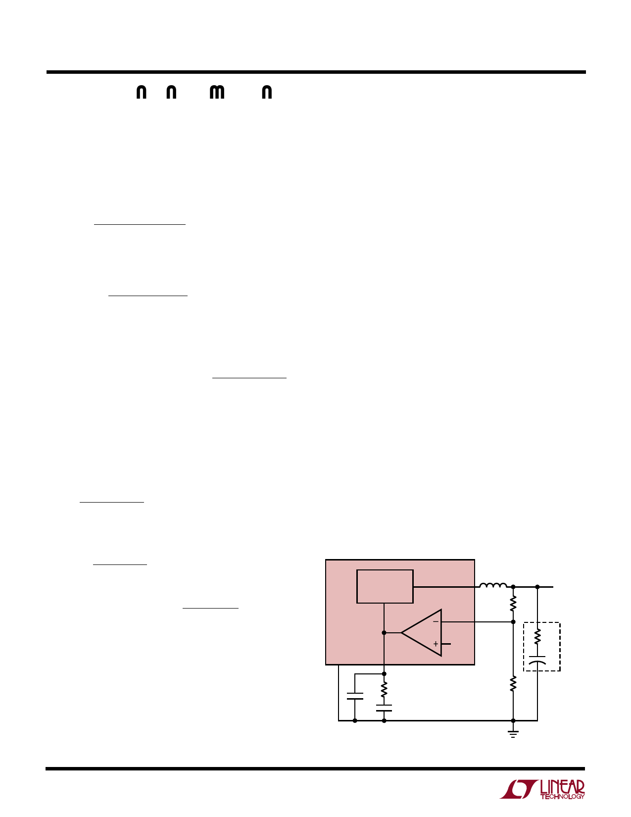
FREQUENCY COMPENSATION
Loop frequency compensation of switching regulators
can be a rather complicated problem because the reactive
components used to achieve high efficiency also
introduce multiple poles into the feedback loop. The
inductor and output capacitor on a conventional step-
down converter actually form a resonant tank circuit that
can exhibit peaking and a rapid 180° phase shift at the
resonant frequency. By contrast, the LT1506 uses a “cur-
rent mode” architecture to help alleviate phase shift cre-
ated by the inductor. The basic connections are shown in
Figure 9. Figure 10 shows a Bode plot of the phase and gain
of the power section of the LT1506, measured from the VC
pin to the output. Gain is set by the 5.3A/V transconduc-
tance of the LT1506 power section and the effective
complex impedance from output to ground. Gain rolls off
smoothly above the 600Hz pole frequency set by the
100µF output capacitor. Phase drop is limited to about
70°. Phase recovers and gain levels off at the zero fre-
quency (≈16kHz) set by capacitor ESR (0.1Ω).
LT1506
CURRENT MODE
POWER STAGE
gm = 5.3A/V
VSW
ERROR
AMPLIFIER
FB
GND
VC
2.42V
RC
CF
CC
OUTPUT
R1
ESR
+
C1
R2
1506 F09
Figure 9. Model for Loop Response
18
Share Link: 