LT1249 Ver la hoja de datos (PDF) - Linear Technology
Número de pieza
componentes Descripción
Fabricante
LT1249 Datasheet PDF : 12 Pages
| |||
LT1249
APPLICATIONS INFORMATION
Line Current Limiting
Maximum voltage across RMOUT is internally limited to
1.1V. Therefore, line current limit is 1.1V divided by the
sense resistor RS. With a 0.2Ω sense resistor RS line
current limit is 5.5A. As a general rule, RS is chosen
according
RS
=
(IM(MAX))(RMOUT )(VLINE(MIN))
K(1.414)POUT(MAX)
where POUT(MAX) is the maximum power output and K is
usually between 1.1 and 1.3 depending on efficiency and
resistor tolerance. When the output is overloaded and line
current reaches limit, output voltage VOUT will drop to keep
line current constant. System stability is still maintained
by the current loop which is controlled by the current
amplifier. Further load current increase results in further
VOUT drop and clipping of the line current, which degrades
power factor.
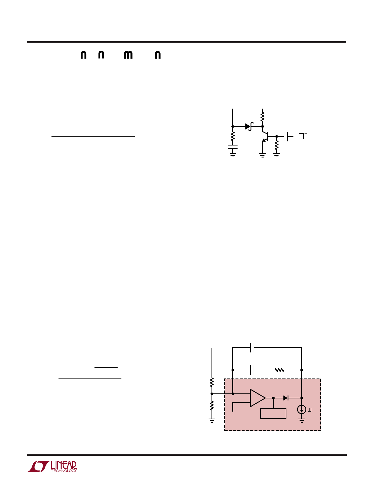
Synchronization
The LT1249 can be externally synchronized in a frequency
range of 127kHz to 160kHz. Figure 2 shows the synchro-
nizing circuit. Synchronizing occurs when CAOUT pin is
pulled below 0.5V with an external transistor and a Schottky
diode. The Schottky diode and the 10k pull-up resistor are
necessary for the required fast slewing back up to the
normal operating voltage on CAOUT after the transistor is
turned off. Positive slewing on CAOUT should be faster
than the oscillator ramp rate of 0.5V/µs.
The width of the synchronizing pulse should be under
60ns. The synchronizing pulses introduce an offset volt-
age on the current amplifier inputs, according to:
∆VOS
=
(ts)(fs)IC
+
VC − 0.5
R2
gm
ts = pulse width
fs = pulse frequency
IC = CAOUT source current (≈ 150µA)
VC = CAOUT operating voltage (1.8V to 6.8V)
R2 = resistorfor the midfrequency “zero” in the current loop
gm = current amplifier transconductance (≈ 320µmho)
With ts = 30ns, fs = 130kHz, VC = 3V and R2 = 10k, offset
voltage shift is ≈5mV. Note that this offset voltage will add
slight distortion to line current at light load.
CAOUT
VCC
R1
1N5712 10k
R2
10k
2N2369
1nF
80pF
2k
5V
0V
1249 F02
Figure 2. Synchronizing the LT1249
Overvoltage Protection
In Figure 3, R1 and R2 set the regulator output DC level:
VOUT = VREF[(R1 + R2)/R2]. With R1 = 1M and R2 = 20k,
VOUT is 382V.
Because of the slow loop response necessary for power
factor correction, output overshoot can occur with sudden
load removal or reduction. To protect the power compo-
nents and output load, the LT1249 voltage error amplifier
senses the output voltage and quickly shuts off the current
switch when overvoltage occurs. When overshoot occurs
on VOUT, the overcurrent from R1 will go through VAOUT
because amplifier feedback keeps VSENSE locked at 7.5V.
When this overcurrent reaches 44µA amplifier sinking
limit, the amplifier loses feedback and its output snaps low
to turn the multiplier off.
Overvoltage trip level: ∆VOUT = (44µA)(R1)
VOUT
0.047µF
C1
0.47µF
R3
330k
R1
1M
VSENSE
R2
20k
VREF
7.5V
–
VAOUT
EA
+
MULTIPLIER
44µA
22µA
LT1249
1249 F03
Figure 3. Overvoltage Protection
7
Share Link: 