LT1248 Ver la hoja de datos (PDF) - Linear Technology
Número de pieza
componentes Descripción
Fabricante
LT1248 Datasheet PDF : 12 Pages
| |||
LT1248
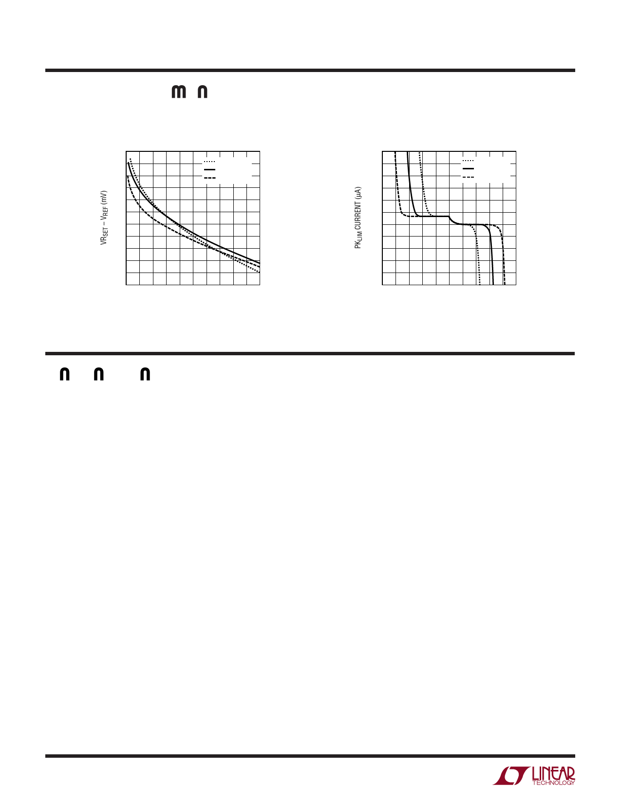
TYPICAL PERFOR A CE CHARACTERISTICS
RSET Voltage vs Current
120
100
TJ = 125°C
80
TJ = 25°C
TJ = –55°C
60
40
20
0
–20
–40
–60
–80
–100
0
–0.2 –0.4 –0.6 –0.8 –1.0
RSET CURRENT (mA)
1248 G16
PKLIM Pin Characteristics
–360
–300
–240
–180
TJ = 125°C
TJ = 25°C
TJ = –55°C
–120
– 60
0
60
120
180
240
300
–0.8
–0.4
0
0.4
PKLIM VOLTAGE (V)
0.8
1248 G17
PI FU CTIO S
Pin 1 (GND).
Pin 2 (PKLIM): The threshold of the peak current limit
comparator is GND. To set current limit, a resistor divider
can be connected from VREF to current sense resistor.
Pin 3 (CAOUT): This is the output of the current amplifier
that senses and forces the line current to follow the
reference signal that comes from the multiplier by com-
manding the pulse width modulator. When CAOUT is low,
the modulator has zero duty cycle.
Pin 4 (ISENSE): This is the inverting input of the current
amplifier. This pin is clamped at – 0.6V by an ESD protec-
tion diode.
Pin 5 (MOUT): This is the multiplier high impedance
current output and the noninverting input of the current
amplifier. This pin is clamped at – 0.6V and 2V.
Pin 6 (IAC): This is the AC line voltage sensing input to the
multiplier. It is a current input that is biased at 2V to
minimize the crossover dead zone caused by low line
voltage. At the pin, a 32k resistor is in series with the
current input, so that a lowpass RC can be used to filter out
the switching noise from the high impedance lines.
Pin 7 (VAOUT): This is the output of the voltage error
amplifier. The output is clamped at 13.5V. When the
output goes below 2.5V, the multiplier output current is
zero.
Pin 8 (OVP): This is the input to the overvoltage compara-
tor. The threshold is 1.05 times the reference voltage.
When the comparator trips, the multiplier is quickly inhib-
ited and outputs no current. Figure 4 in the Applications
Information section shows how to set overvoltage thresh-
old with only one additional resistor.
Pin 9 (VREF): This is the 7.5V reference. When either VCC
or EN/SYNC goes low, VREF will stay at 0V. VREF biases
most of the internal circuity and can source up to 5mA
externally.
Pin 10 (EN/SYNC): This pin has two functions. When it
goes below 2.6V, the chip goes into shutdown mode and
draws little current. Pulses at this pin that go below the 5V
threshold will synchronize the chip. The synchronizing
pulses should have an on-time of at least 200ns for the
LT1248 resetting circuit to work.
Pin 11 (VSENSE): This is the inverting input to the voltage
amplifier.
6
Share Link: 