LS7535(1996) Ver la hoja de datos (PDF) - LSI Corporation
Número de pieza
componentes Descripción
Fabricante
LS7535 Datasheet PDF : 8 Pages
| |||
SYNC 4
CAP 3
DOZE 2
DOWN 6
UP 5
VSS 1
VDD 7
BUF
BUF
BUF
BUF
(+V)
(-V)
PHASE
LOCK
LOOP
CONTROL
LOGIC
BRIGHTNESS
MEMORY
Ø
POINTER
DIGITAL
COM-
PARATOR
OUTPUT
DRIVER
8 TRIG
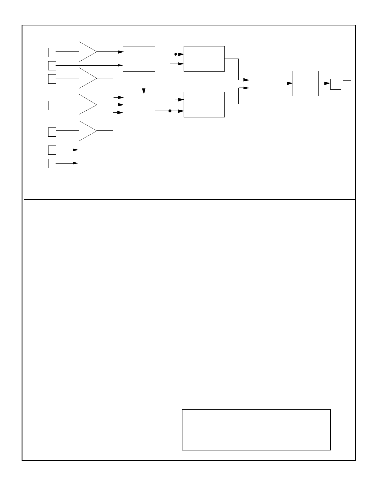
FIGURE 4
LS7534/LS7535 BLOCK DIAGRAM
APPLICATION EXAMPLES:
Typical dimmer light switch circuit schematics are shown in Fig. 5A (LS7534) and
Fig. 5B (LS7535). The brightness of the lamp is set by touching the UP and DOWN
touch plates in Fig. 5A and closure of the UP and DOWN switches in Fig. 5B. The
functions of different components are as follows:
• Z, D1, R1, C2 and C5 produce the 15V DC supply for the chip.
• R2 and C4 filter and current limit the AC signal for the SYNC input.
• C3 is the filter capacitor for the internal PLL.
• C1 and L are RFI filters.
• In Fig. 5A, R3 and R4 set the touch sensitivity of the UP and DOWN inputs.
• In Fig. 5B, R3 limits the current between Vss and the UP and DOWN inputs upon
closure of a switch.
• The resistor and diode connected between the chip output and the triac gate
provides current limiting and isolation for the chip. The resistor is R5 in Fig. 5A
and R4 in Fig. 5B.
• In Fig. 5B, PCB layout may cause triac switching transients to be coupled to the UP
or Down input which can have the effect of having a Long switch closure “lock-up”
at a certain phase angle output. In this case, capacitors C6 and C7 must be added
as shown.
7534/35-080796-5
The information included herein is believed to be
accurate and reliable. However, LSI Computer Systems,
Inc. assumes no responsibilities for inaccuracies, nor for
any infringements of patent rights of others which may
result from its use.
Share Link: 