LR1107L-XX-AB3-D-R Ver la hoja de datos (PDF) - Unisonic Technologies
Número de pieza
componentes Descripción
Fabricante
LR1107L-XX-AB3-D-R Datasheet PDF : 6 Pages
| |||
LR1107/E
CMOS IC
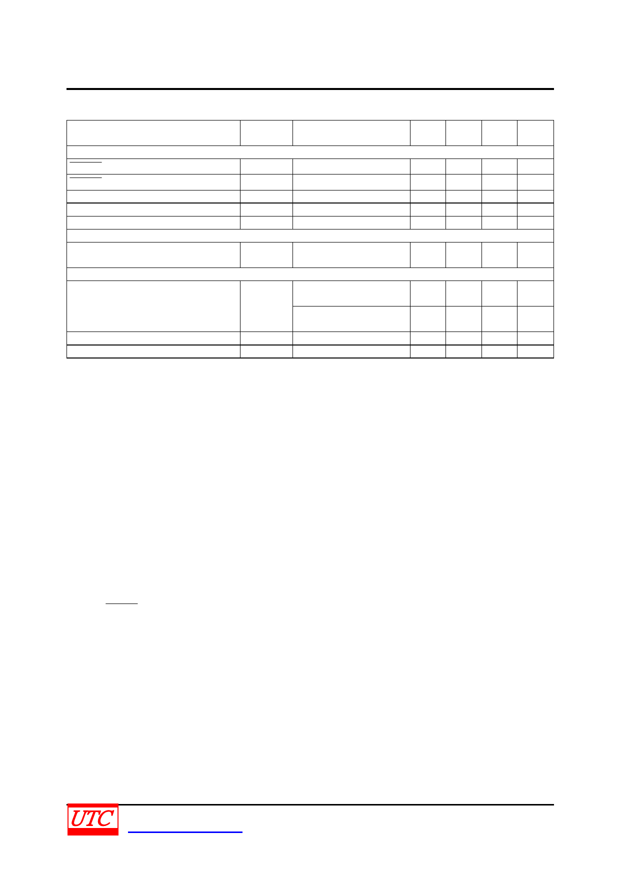
ELECTRICAL CHARACTERISTICS(Cont.)
PARAMETER
SYMBOL TEST CONDITIONS
ERROR FLAG COMPARATOR (for LR1107E)
ERROR Flag Saturation
VEF(SAT)
ERROR Flag Pin Leakage Current
II(LEAK)
Threshold
Threshold Hysteresis
Flag Reset Delay
SET/ADJ Mode (for LR1107 5pins)
VT
VTHR
tD
SET Voltage
VSET
AC PARAMETERS
Ripple Rejection
PSRR
Output Noise Density
Output Noise Voltage
ρn(l/f)
eN
ISINK = 100μA
(Note 7)
(Note 7)
Measured on ADJ,
IOUT =10mA
VIN = VOUT + 1.5V
COUT=100uF, VOUT = 3.3V
VIN = VOUT + 0.3V
COUT=100uF, VOUT = 3.3V
f = 120Hz
BW = 10Hz – 100kHz
TYP
MIN
MAX UNIT
(Note 3)
0.02 0.1
V
1
nA
5
7
16
%
2
4.2
8
%
17
μs
1.110 1.145 1.188 V
60
dB
40
dB
0.8
μV
150
μVrms
Note 1. Absolute maximum ratings are those values beyond which the device could be permanently damaged.
Absolute maximum ratings are stress ratings only and functional device operation is not implied. Conditions
for which the device is intended to be functional is indicated by operating ratings, but specific performance
limits isn’t be guaranteed. To make sure of specifications and test conditions, read Electrical Characteristics.
Only for the test conditions listed the guaranteed specifications can be applied. When the device is not
operated under the listed test conditions some performance characteristics may degrade.
2. Devices must be derated based on package thermal resistance at elevated temperatures.
3. The most likely parametric norm represents at 25°C.
4. The LR1107/E output must be diode-clamped to ground. If used in a dual-supply system where the regulator
load is returned to a negative supply.
5. Between the VIN and VOUT terminals the output PMOS structure contains a diode. This diode is reverse
biased normally. If the voltage at the output terminal is forced to be higher than the voltage at the input
terminal this diode will get forward biased. This diode can withstand 650mA of peak current and 120mA of
DC current typically.
6. Output voltage line regulation is the change in output voltage from the nominal value which is due to change
in the input line voltage. Which is defined as the change in output voltage from the nominal value due to
change in load current is output voltage load regulation. The load regulation and line regulation specification
include the typical number only. But, the limits for load and line regulation are included in the output voltage
tolerance specification.
7. ERROR Flag hysteresis and threshold are specified as regulated output voltage’s percentage.
8. At which the output drops 2% below the normal value dropout voltage is defined as the minimum input to
output differential voltage. Only to output voltages of 2.5V and above dropout voltage specification applies.
For output voltages below 2.5V, since the minimum input voltage is 2.5V, the drop-out voltage is nothing but
the input to output differential.
9. Specification has been tested at −40°C≤TJ≤ 85°C cause under shutdown conditions the temperature rise of
the device is negligible.
10. The minimum operating VIN value is equal to VOUT(NOM) + VDROPOUT] or 2.5V, just the greater.
UNISONIC TECHNOLOGIES CO., LTD
www.unisonic.com.tw
5 of 6
QW-R102-033.H
Share Link: 