L99H01 Ver la hoja de datos (PDF) - STMicroelectronics
Número de pieza
componentes Descripción
Fabricante
L99H01 Datasheet PDF : 53 Pages
| |||
L99H01
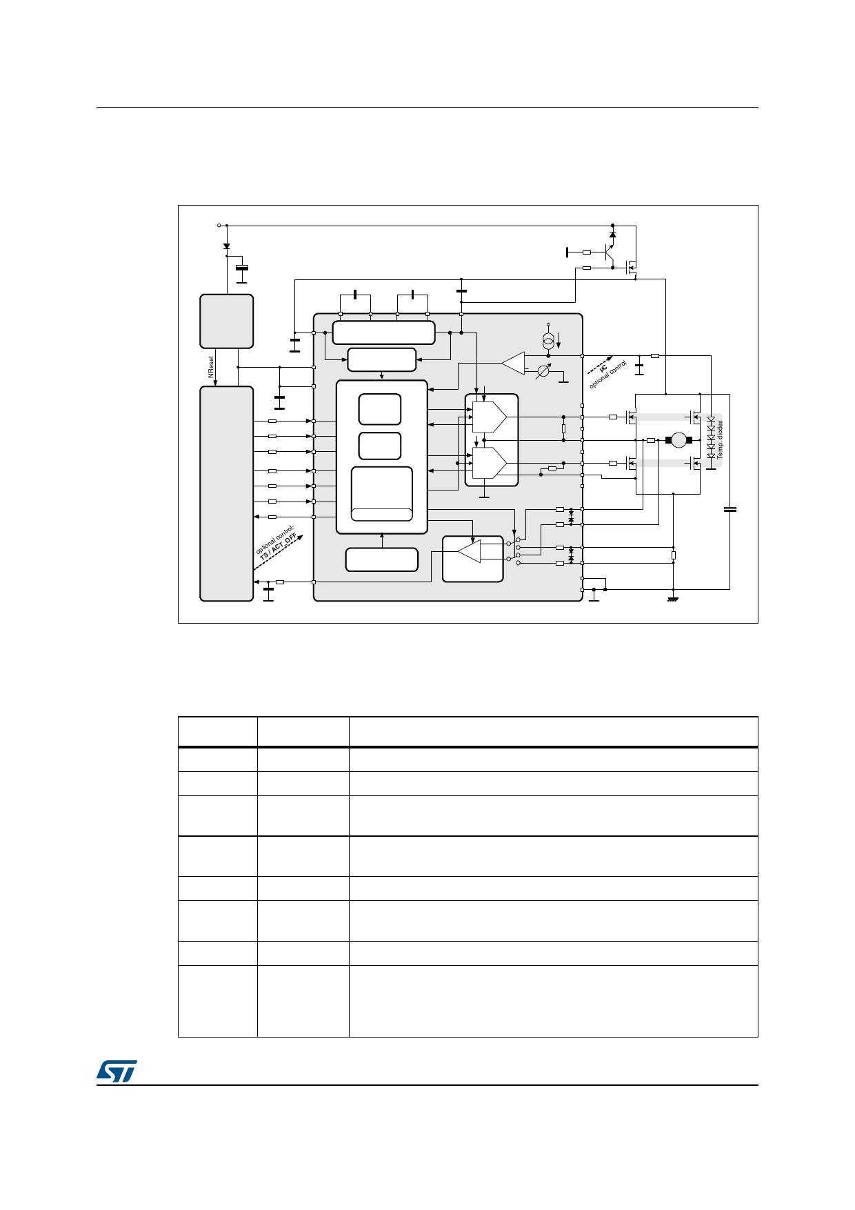
Block diagram and pin description
1
Block diagram and pin description
Figure 1. Block diagram
6"!4
1.1
95(*
6��
6
N&
N&
N&
&3 &3 &3 &3
&3
9FF
9V
&HQWUDO6WHS&KDUJH3XPS
9FF
9FFG
&
(1
',5
3:0
&61
&/.
',
'2
OP7TI6ON A$L�&CO7NBT2RO)L)
&62
8QGHUYROWDJH
2YHUYROWDJH'HW
&RQWURO/RJLF
:DNHXS
IURP
6OHHSPRGH
026)(7
&RQWURO
63,
,QWHUIDFH
:DWFK'RJ
7HPSHUDWXUH3UHZDUQLQJ
7HPSHUDWXUH6KXWGRZQ
9&3
9V
&RQWURO
'LDJQRVLV
&RQWURO
'LDJQRVLV
'ATE
$RIVER
(3
9&3
'ATE
$RIVER
,3
X�
3URJUDPPDEOH
9'67+ W'HDG
&XUUHQW6HQVH08;
3URJUDPPDEOH
*DLQ
'LIIHUHQWLDO&XUUHQW
6HQVH$PSOLILHU
76
$&7B2))
OPTION&AL�CONTROL
*+
*+
6+
6+
*/
*/
6/
6/
&6,
&6,
&6,
&6,
*1'
*1''
-
("1($'5
Pinout PowerSSO-36
Table 2. Pin definitions and functions
Pin
Symbol
Function
1
GND
Ground. Reference potential, connected to slug.
2
GNDD Digital ground. Reference potential.
3
VCCD
Logic voltage supply 3.3 V/5 V: for this input a ceramic capacitor as
close as possible to GND is recommended.
4
VCC
Analog voltage supply 3.3 V/5 V: for this input a ceramic capacitor as
close as possible to GND is recommended.
5
EN
Enable input. The enable input has a pull-down resistor.
6
DIR
Direction select input for H-bridge control. This input has a pull-down
current.
7
PWM
PWM input for H-bridge control. This input has a pull-down current.
Chip select not input: this input is low active and requires CMOS logic
8
CSN
levels. The serial data transfer between L99H01 and microcontroller is
enabled by pulling the input CSN to low-level. This input has a pull-up
current.
DocID15567 Rev 5
7/53
52
Share Link: 