LP2951CD Ver la hoja de datos (PDF) - ON Semiconductor
Número de pieza
componentes Descripción
Fabricante
LP2951CD Datasheet PDF : 22 Pages
| |||
LP2950, LP2951, NCV2951
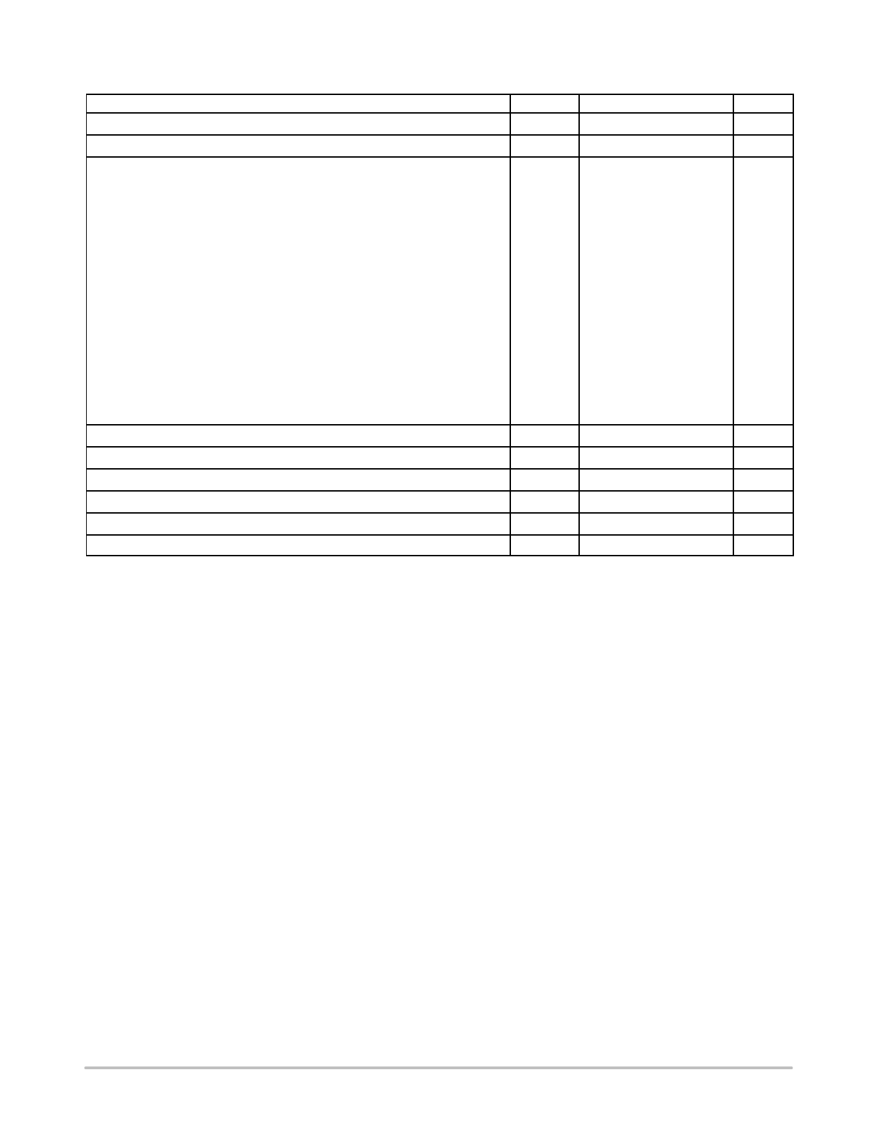
MAXIMUM RATINGS (TA = 25C, unless otherwise noted.)
Rating
Symbol
Value
Unit
Input Voltage
VCC
30
Vdc
ÁÁÁÁÁÁÁÁÁÁÁÁÁÁÁÁÁÁÁÁÁÁÁÁÁÁÁÁÁÁÁÁÁ Peak Transient Input Voltage (t < 20 ms)
Power Dissipation and Thermal Characteristics
VCC
32
Vdc
Maximum Power Dissipation
PD
Internally Limited
W
Case 751(SOIC−8) D Suffix
Thermal Resistance, Junction−to−Ambient
Thermal Resistance, Junction−to−Case
RqJA
RqJC
180
C/W
45
C/W
Case 369A (DPAK) DT Suffix (Note 1)
Thermal Resistance, Junction−to−Ambient
Thermal Resistance, Junction−to−Case
RqJA
RqJC
92
C/W
6.0
C/W
Case 29 (TO−226AA/TO−92) Z Suffix
Thermal Resistance, Junction−to−Ambient
Thermal Resistance, Junction−to−Case
RqJA
RqJC
160
C/W
83
C/W
Case 626 N Suffix
Thermal Resistance, Junction−to−Ambient
RqJA
105
C/W
Case 846A (Micro8) DM Suffix
Thermal Resistance, Junction−to−Ambient
RqJA
240
C/W
Feedback Input Voltage
Vfb
−1.5 to +30
Vdc
Shutdown Input Voltage
Vsd
−0.3 to +30
Vdc
Error Comparator Output Voltage
Verr
−0.3 to +30
Vdc
Operating Ambient Temperature Range
TA
−40 to +125
C
Maximum Die Junction Temperature Range
TJ
+150
C
Storage Temperature Range
Tstg
−65 to +150
C
Stresses exceeding Maximum Ratings may damage the device. Maximum Ratings are stress ratings only. Functional operation above the
Recommended Operating Conditions is not implied. Extended exposure to stresses above the Recommended Operating Conditions may affect
device reliability.
http://onsemi.com
3
Share Link: 