LP2951CD(2006) Ver la hoja de datos (PDF) - ON Semiconductor
Número de pieza
componentes Descripción
Fabricante
LP2951CD Datasheet PDF : 24 Pages
| |||
LP2950, LP2951, NCV2951
100 mA, Low Power Low
Dropout Voltage Regulator
The LP2950 and LP2951 are micropower voltage regulators that are
specifically designed to maintain proper regulation with an extremely
low input−to−output voltage differential. These devices feature a very
low quiescent bias current of 75 mA and are capable of supplying
output currents in excess of 100 mA. Internal current and thermal
limiting protection is provided.
The LP2951 has three additional features. The first is the Error
Output that can be used to signal external circuitry of an out of
regulation condition, or as a microprocessor power−on reset. The
second feature allows the output voltage to be preset to 5.0 V, 3.3 V or
3.0 V output (depending on the version) or programmed from 1.25 V
to 29 V. It consists of a pinned out resistor divider along with direct
access to the Error Amplifier feedback input. The third feature is a
Shutdown input that allows a logic level signal to turn−off or turn−on
the regulator output.
Due to the low input−to−output voltage differential and bias current
specifications, these devices are ideally suited for battery powered
computer, consumer, and industrial equipment where an extension of
useful battery life is desirable. The LP2950 is available in the three
pin case 29 and DPAK packages, and the LP2951 is available in the
eight pin dual−in−line, SOIC−8 and Micro8 surface mount packages.
The ‘A’ suffix devices feature an initial output voltage tolerance
± 0.5%.
Features
• Pb−Free Packages are Available
• Low Quiescent Bias Current of 75 mA
• Low Input−to−Output Voltage Differential of 50 mV at 100 mA and
380 mV at 100 mA
• 5.0 V, 3.3 V or 3.0 V ±0.5% Allows Use as a Regulator or Reference
• Extremely Tight Line and Load Regulation
• Requires Only a 1.0 mF Output Capacitor for Stability
• Internal Current and Thermal Limiting
• NCV Prefix for Automotive and Other Applications Requiring Site
and Control Changes
LP2951 Additional Features
• Error Output Signals an Out of Regulation Condition
• Output Programmable from 1.25 V to 29 V
• Logic Level Shutdown Input
(See Following Page for Device Information.)
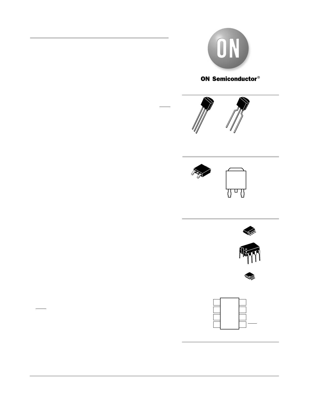
http://onsemi.com
TO−92
Z SUFFIX
CASE 29
1
23
Pin: 1. Output
2. Ground
3. Input
DPAK
DT SUFFIX
CASE 369C
4
12
3
PIN CONNECTIONS
12 3
Pin: 1. Input
2. Ground
3. Output
(Top View)
Heatsink surface (shown as terminal 4 in
case outline drawing) is connected to Pin 2.
SOIC−8
D SUFFIX
CASE 751
8
1
PDIP−8
N SUFFIX
CASE 626
Micro8E
DM SUFFIX
CASE 846A
8
1
8
1
PIN CONNECTIONS
Output 1
Sense 2
Shutdown 3
GND 4
8 Input
7 Feedback
6 VO Tap
5 Error Output
(Top View)
ORDERING & MARKING INFORMATION
See detailed ordering and shipping information in the package
dimensions section on pages 14 and 16 of this data sheet.
See general marking information in the device marking
section on page 18 of this data sheet.
© Semiconductor Components Industries, LLC, 2006
1
December, 2006 − Rev. 19
Publication Order Number:
LP2950/D
Share Link: 