LH28F800BJB-PTTL10 Ver la hoja de datos (PDF) - Sharp Electronics
Número de pieza
componentes Descripción
Fabricante
LH28F800BJB-PTTL10 Datasheet PDF : 47 Pages
| |||
LHF80J22
6
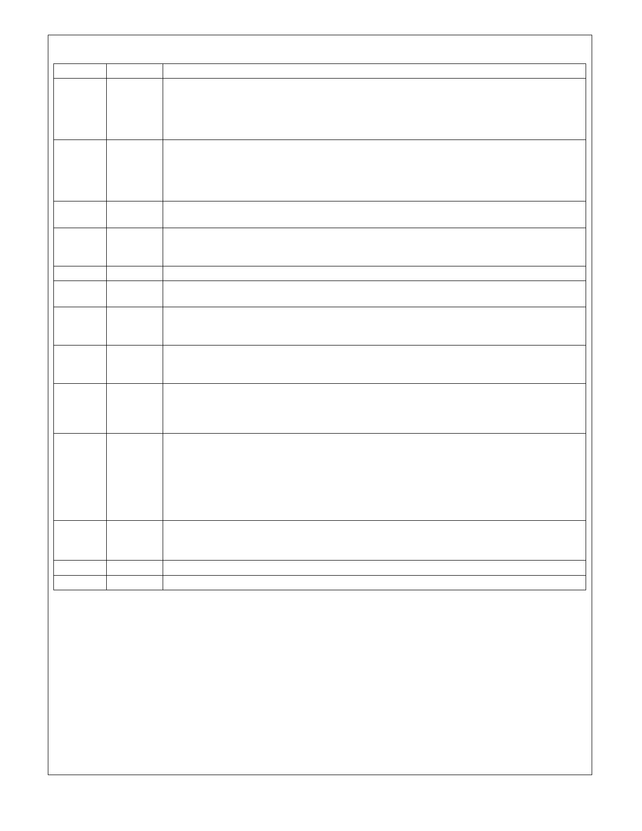
Symbol
A-1
A0-A18
DQ0-DQ15
CE#
RP#
OE#
WE#
WP#
BYTE#
RY/BY#
VCCW
VCC
GND
NC
Type
INPUT
INPUT/
OUTPUT
INPUT
INPUT
INPUT
INPUT
INPUT
INPUT
OPEN
DRAIN
OUTPUT
SUPPLY
SUPPLY
SUPPLY
Table 1. Pin Descriptions
Name and Function
ADDRESS INPUTS: Inputs for addresses during read and write operations. Addresses are
internally latched during a write cycle.
A-1: Lower address input while BYTE# is VIL. A-1 pin changes DQ15 pin while BYTE# is VIH.
A15-A18: Main Block Address.
A12-A18: Boot and Parameter Block Address.
DATA INPUT/OUTPUTS: Inputs data and commands during CUI write cycles; outputs data
during memory array, status register and identifier code read cycles. Data pins float to high-
impedance when the chip is deselected or outputs are disabled. Data is internally latched during a
write cycle. DQ8-DQ15 pins are not used while byte mode (BYTE#=VIL). Then, DQ15 pin
changes A-1 address input.
CHIP ENABLE: Activates the device’s control logic, input buffers, decoders and sense amplifiers.
CE#-high deselects the device and reduces power consumption to standby levels.
RESET: Resets the device internal automation. RP#-high enables normal operation. When driven
low, RP# inhibits write operations which provides data protection during power transitions. Exit
from reset mode sets the device to read array mode. RP# must be VIL during power-up.
OUTPUT ENABLE: Gates the device’s outputs during a read cycle.
WRITE ENABLE: Controls writes to the CUI and array blocks. Addresses and data are latched on
the rising edge of the WE# pulse.
WRITE PROTECT: When WP# is VIL, boot blocks cannot be written or erased. When WP# is
VIH, locked boot blocks can not be written or erased. WP# is not affected parameter and main
blocks.
BYTE ENABLE: BYTE# VIL places device in byte mode (×8). All data is then input or output on
DQ0-7, and DQ8-15 float. BYTE# VIH places the device in word mode (×16), and turns off the A-1
input buffer.
READY/BUSY#: Indicates the status of the internal WSM. When low, the WSM is performing an
internal operation (block erase, full chip erase, word/byte write or lock-bit configuration).
RY/BY#-high Z indicates that the WSM is ready for new commands, block erase is suspended,
and word/byte write is inactive, word/byte write is suspended, or the device is in reset mode.
BLOCK ERASE, FULL CHIP ERASE, WORD/BYTE WRITE OR LOCK-BIT
CONFIGURATION POWER SUPPLY: For erasing array blocks, writing words/bytes or
configuring lock-bits. With VCCW≤VCCWLK, memory contents cannot be altered. Block erase, full
chip erase, word/byte write and lock-bit configuration with an invalid VCCW (see 6.2.3 DC
Characteristics) produce spurious results and should not be attempted. Applying 12V±0.3V to
VCCW during erase/write can only be done for a maximum of 1000 cycles on each block. VCCW
may be connected to 12V±0.3V for a total of 80 hours maximum.
DEVICE POWER SUPPLY: Do not float any power pins. With VCC≤VLKO, all write attempts to
the flash memory are inhibited. Device operations at invalid VCC voltage (see 6.2.3 DC
Characteristics) produce spurious results and should not be attempted.
GROUND: Do not float any ground pins.
NO CONNECT: Lead is not internal connected; it may be driven or floated.
Rev. 1.27
Share Link: 