LH28F640SP Ver la hoja de datos (PDF) - Sharp Electronics
NГәmero de pieza
componentes DescripciГіn
Fabricante
LH28F640SP Datasheet PDF : 45 Pages
| |||
LHF64P01
4
Symbol
A0
A22-A1
DQ15-DQ0
CE0,
CE1,
CE2
RP#
OE#
WE#
STS
BYTE#
VPEN
VCC
VCCQ
GND
NC
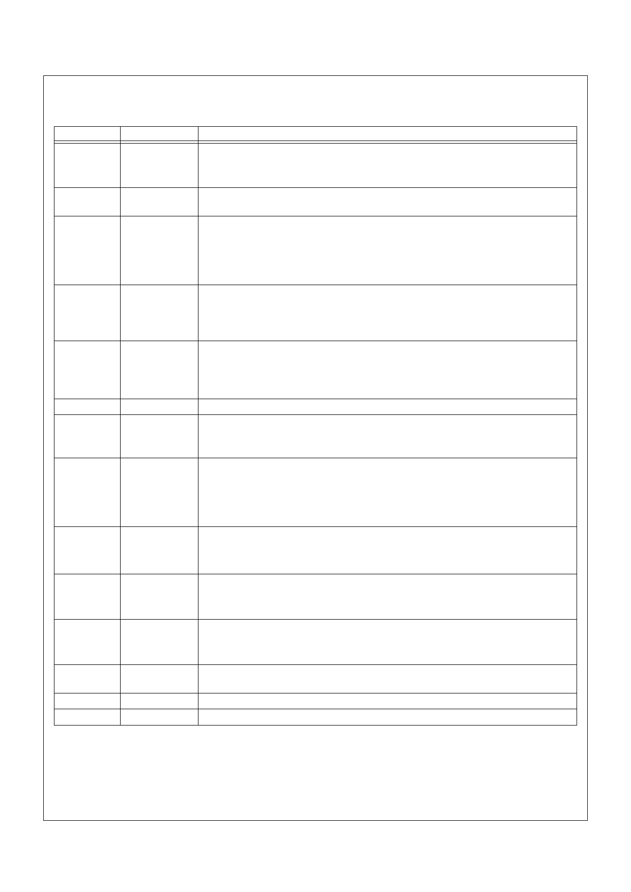
Table 1. Pin Descriptions
Type
Name and Function
INPUT
ADDRESS INPUTS: Lowest address input in byte mode (BYTE#=VIL : Г—8 bit).
Address is internally latched during an erase or a program cycle. This pin is not used in
word mode (BYTE#=VIH : Г—16 bit)
INPUT
ADDRESS INPUTS: Inputs for addresses during read, erase and program operations.
Addresses are internally latched during an erase or a program cycle.
INPUT/
OUTPUT
DATA INPUTS/OUTPUTS: Inputs data and commands during CUI (Command User
Interface) write cycles, outputs data during memory array, status register, query code,
identifier code reads. Data pins float to high-impedance (High Z) when the chip or
outputs are deselected. Data is internally latched during an erase or program cycle.
DQ15-DQ8 pins are not used in byte mode (BYTE#=VIL : Г—8 bit).
INPUT
CHIP ENABLE: Activates the deviceвҖҷs control logic, input buffers, decoders and sense
amplifiers. When the device is de-selected, power consumption reduces to standby
levels. Refer to Table 2 to determine whether the device is selected or de-selected
depending on the state of CE0, CE1 and CE2.
INPUT
RESET: When low (VIL), RP# resets internal automation and inhibits erase and program
operations, which provides data protection. RP#-high (VIH) enables normal operation.
After power-up or reset mode, the device is automatically set to read array mode.
RP# must be low during power-up/down.
INPUT OUTPUT ENABLE: Gates the deviceвҖҷs outputs during a read cycle.
INPUT
WRITE ENABLE: Controls writes to the CUI and array blocks. Addresses and data are
latched on the first edge of CE0, CE1 or CE2 that disables the device or the rising edge of
WE# (whichever occurs first).
OPEN DRAIN
OUTPUT
STATUS: Indicates the status of the internal WSM (Write State Machine). When
configured in level mode (default mode), STS acts as a RY/BY# pin (STS is VOL when
the WSM is executing internal erase or program algorithms). When configured in one of
its pulse modes, STS can pulse to indicate erase/program completion. Refer to Table 9
for STS configuration.
INPUT
BYTE ENABLE: BYTE# VIL places the device in byte mode (Г—8). In this mode, DQ15-
DQ8 is floated (High Z) and A0 is the lowest address input. BYTE# VIH places the
device in word mode (Г—16) and A1 is the lowest address input.
INPUT
MONITORING POWER SUPPLY VOLTAGE: VPEN is not used for power supply pin.
With VPENвүӨVPENLK, block erase, (page buffer) program, block lock configuration and
OTP program cannot be executed and should not be attempted.
SUPPLY
DEVICE POWER SUPPLY (2.7V-3.6V): With VCCвүӨVLKO, all write attempts to the
flash memory are inhibited. Device operations at invalid VCC voltage (refer to DC
Characteristics) produce spurious results and should not be attempted.
SUPPLY
INPUT/OUTPUT POWER SUPPLY (2.7V-3.6V): Power supply for all input/output
pins.
SUPPLY GROUND: Do not float any ground pins.
NO CONNECT: Lead is not internally connected; it may be driven or floated.
Rev. 0.06
Share Link: 